
Data Sheet

Analog Integrated Circuit Device Data
Freescale Semiconductor 15
33926
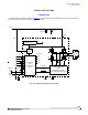
FUNCTIONAL INTERNAL BLOCK DESCRIPTION
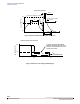
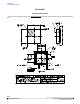
FUNCTIONAL PIN DESCRIPTION
FUNCTIONAL INTERNAL BLOCK DESCRIPTION
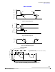
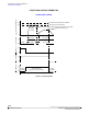
Figure 10. 33926 Functional Internal Block Diagram
ANALOG CONTROL AND PROTECTION CIRCUITRY
The on-chip voltage regulator supplies 3.3 V to the internal logic. The charge pump provides gate drive for the H-Bridge
MOSFETs. The current and temperature sense circuitry provides detection and protection for the output drivers. Output
undervoltage protection shuts down the MOSFETS.
GATE CONTROL LOGIC
The 33926 is a monolithic H-Bridge Power IC designed primarily for any low voltage DC servo motor control application within
the current and voltage limits stated for the device. Two independent inputs provide polarity control of two half-bridge totem-pole
outputs. Two independent disable inputs are provided to force the H-Bridge outputs to tri-state (high-impedance off-state).
H-BRIDGE OUTPUT DRIVERS: OUT1 AND OUT2
The H-Bridge is the power output stage. The current flow from OUT1 to OUT2 is reversible and under full control of the user
by way of the Input Control Logic. The output stage is designed to produce full load control under all system conditions. All
protective and control features are integrated into the control and protection blocks. The sensors for current and temperature are
integrated directly into the output MOSFET for maximum accuracy and dependability.
MCU
INTERFACE
PROTECTION LOGIC CONTROL
COMMAND AND FAULT REGISTERS
GATE CONTROL LOGIC
CURRENT SENSE
VOLTAGE
REGULATION
TEMPERATURE
SENSE
CHARGE
PUMP
H-BRIDGE
OUTPUT DRIVERS
OUT1 - OUT2
ANALOG CONTROL AND PROTECTION
PWM CONTROLLER