
Data Sheet

Analog Integrated Circuit Device Data
14 Freescale Semiconductor
33926
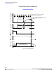
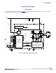
FUNCTIONAL DESCRIPTION
FUNCTIONAL PIN DESCRIPTION
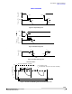
INPUT 1,2 AND DISABLE INPUT 1,2 (IN1, IN2, AND D1, D2)
These pins are input control pins used to control the outputs. These pins are 3.0 V/ 5.0 V CMOS-compatible inputs with
hysteresis. IN1 and IN2 independently control OUT1 and OUT2, respectively. D1 and
D2 are complementary inputs used to tri-
state disable the H-Bridge outputs.
When either D1 or D2 is SET (D1 = logic HIGH or D2 = logic LOW) in the disable state, outputs OUT1 and OUT2 are both tri-
state disabled; however, the rest of the device circuitry is fully operational and the supply I
PWR(STANDBY)
current is reduced to a
few mA. Refer to
Table 4, Static Electrical Characteristics, page 8.
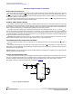
H-BRIDGE OUTPUT (OUT1, OUT2)
These pins are the outputs of the H-Bridge with integrated freewheeling diodes. The bridge output is controlled using the IN1,
IN2, D1, and D2 inputs. The outputs have PWM current limiting above the I
LIM
threshold. The outputs also have thermal shutdown
(tri-state latch-OFF) with hysteresis as well as short-circuit latch-OFF protection.
A disable timer (time t
B
) is incorporated to distinguish between load currents that are higher than the I
LIM
threshold and short-
circuit currents. This timer is activated at each output transition.
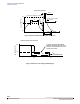
CHARGE PUMP CAPACITOR (CCP)
This pin is the charge pump output pin and connection for the external charge pump reservoir capacitor. The allowable value
is from 30 to 100 nF. This capacitor must be connected from the CCP pin to the VPWR pin. The device cannot operate properly
without the external reservoir capacitor.
ENABLE INPUT (EN)
The EN pin is used to place the device in a Sleep mode so as to consume very low currents. When the EN pin voltage is a
logic LOW state, the device is in Sleep mode. The device is enabled and fully operational when the EN pin voltage is in logic
HIGH. An internal pulldown resistor maintains the device in Sleep mode in the event EN is driven through a high-impedance I/O,
or an unpowered microcontroller, or the EN input becomes disconnected.
FEEDBACK (FB)
The 33926 has a feedback output (FB) for “real time” monitoring of H-Bridge high-side output currents to facilitate closed-loop
operation for motor speed and torque control.
The FB pin provides current sensing feedback of the H-Bridge high-side drivers. When running in the forward or reverse
direction, a ground-referenced 0.24% of load current is output to this pin. Through the use of an external resistor to ground, the
proportional feedback current can be converted to a proportional voltage equivalent and the controlling microcontroller can “read”
the current proportional voltage with its analog-to-digital converter (ADC). This is intended to provide the user with only first-order
motor current feedback for motor torque control. The resistance range for the linear operation of the FB pin is 100
< R
FB
< 300 .
If PWM-ing is implemented using the disable pin inputs (either D1 or D2), a small filter capacitor (~1.0 µF) may be required in
parallel with the R
FB
resistor to ground for spike suppression.