
Data Sheet

Analog Integrated Circuit Device Data
Freescale Semiconductor 13
33926
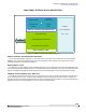
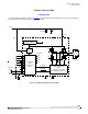
FUNCTIONAL DESCRIPTION
INTRODUCTION
FUNCTIONAL DESCRIPTION
INTRODUCTION
Numerous protection and operational features (speed, torque, direction, dynamic breaking, PWM control, and closed-loop
control) make the 33926 a very attractive, cost-effective solution for controlling a broad range of small DC motors. The 33926
outputs are capable of supporting peak DC load currents of up to 5.0
A from a 28 V
PWR
source. An internal charge pump and
gate drive circuitry are provided that can support external PWM frequencies up to 20 kHz.
The 33926 has an analog feedback (current mirror) output pin (the FB pin) that provides a constant-current source ratioed to
the active high-side MOSFETs’ current. This can be used to provide “real time” monitoring of output current to facilitate closed-
loop operation for motor speed/torque control, or for the detection of open load conditions.
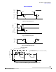
Two independent inputs, IN1 and IN2, provide control of the two totem-pole half-bridge outputs. An input invert, INV, changes
IN1 and IN2 to LOW = true logic. Two different output slew rates are selectable via the SLEW input. Two independent disable
inputs, D1 and D2, provide the means to force the H-Bridge outputs to a high-impedance state (all H-Bridge switches OFF). An
EN pin controls an enable function that allows the IC to be placed in a power-conserving Sleep mode.
The 33926 has Output Current Limiting (via Constant OFF-Time PWM Current Regulation), Output Short-circuit Detection with
Latch-OFF, and Overtemperature Detection with Latch-OFF. Once the device is latched-OFF due to a fault condition, either of
the Disable inputs (D1 or D2), V
PWR
, or EN must be “toggled” to clear the status flag.
Current limiting (Load Current Regulation) is accomplished by a constant-OFF time PWM method using current limit threshold
triggering. The current limiting scheme is unique in that it incorporates a junction temperature-dependent current limit threshold.
This means that the current limit threshold is “reduced to around 4.2
A” as the junction temperature increases above 160 °C.
When the temperature is above 175 °C, overtemperature shutdown (latch-OFF) will occur. This combination of features allows
the device to continue operating for short periods of time (<
30 seconds) with unexpected loads, while still retaining adequate
protection for both the device and the load.
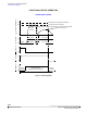
FUNCTIONAL PIN DESCRIPTION
POWER GROUND AND ANALOG GROUND (PGND AND AGND)
The power and analog ground pins should be connected together with a very low-impedance connection.
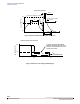
POSITIVE POWER SUPPLY (VPWR)
VPWR pins are the power supply inputs to the device. All VPWR pins must be connected together on the printed circuit board
with as short as possible traces, offering as low-impedance as possible between pins.
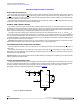
Transients on V
PWR
which go below the undervoltage threshold will result in the protection activating. It is essential to use an
input filter capacitor of sufficient size and low ESR to sustain a V
PWR
greater than V
UVLO
when the load is switched (See 33926
Typical Application Schematic on page 19).
STATUS FLAG (SF)
This pin is the device fault status output. This output is an active LOW open drain structure requiring a pull-up resistor to V
DD
.
The maximum V
DD
is < 7.0 V. Refer to Table 6, Truth Table, page 17 for the SF Output status definition.
INPUT INVERT (INV)
The Input Invert Control pin sets IN1 and IN2 to LOW = TRUE. This is a Schmitt trigger input with ~ 80 µA sink; the default
condition is non-inverted. If IN1 and IN2 are set so that the current is being commanded to flow through the load attached between
OUT1 and OUT2, changing the logic level at INV will have the effect of reversing the direction of current commanded. Thus, the
INV input may be used as a “forward/reverse” command input. If both IN1 and IN2 are the same logic level, then changing the
logic level at INV will have the effect of changing the bridge’s output from freewheeling high to freewheeling low or vice versa.
SLEW RATE (SLEW)
The SLEW pin is the logic input that selects fast or slow slew rate. Schmitt trigger input with ~ 80 µA sink so the default
condition is SLOW. When SLEW is set to SLOW, PWM-ing should be limited to frequencies less than 11
kHz in order to allow
the internal high-side driver circuitry time to fully enhance the high-side MOSFETs.