
Data Sheet

Analog Integrated Circuit Device Data
10 Freescale Semiconductor
33926
ELECTRICAL CHARACTERISTICS
DYNAMIC ELECTRICAL CHARACTERISTICS
DYNAMIC ELECTRICAL CHARACTERISTICS
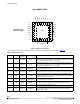
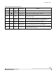
Table 5. Dynamic Electrical Characteristics
Characteristics noted under conditions 5.0 V V
PWR
28 V, - 40 C T
A
125 C, GND = 0 V, unless otherwise noted. Typical
values noted reflect the approximate parameter means at T
A
= 25 °C under nominal conditions, unless otherwise noted.
Symbol Characteristic Min Typ Max Unit Notes
TIMING CHARACTERISTICS
f
PWM
PWM Frequency
– – 20 kHz
(21)
f
MAX
Maximum Switching Frequency During Current Limit Regulation
– – 20 kHz
(22)
t
DON
Output ON Delay
V
PWR
= 14 V
– – 18
s
(23)
t
DOFF
Output OFF Delay
V
PWR
= 14 V
– – 12
s
(23)
t
A
I
LIM
Output Constant-OFF Time
15 20.5 32
s
(24)
t
B
I
LIM
Blanking Time
12 16.5 27
s
(25)
t
DDISABLE
Disable Delay Time
– – 8.0 s
(26)
t
F
, t
R
Output Rise and Fall Time
SLEW = SLOW
SLEW = FAST
1.5
0.2
3.0
–
6.0
1.45
s
(27)
t
FAULT
Short-circuit / Overtemperature Turn-OFF (Latch-OFF) Time
– – 8.0 s
(28)
(29)
t
POD
Power-ON Delay Time
– 1.0 5.0 ms
(29)
t
R R
Output MOSFET Body Diode Reverse Recovery Time
75 100 150
ns
(29)
f
CP
Charge Pump Operating Frequency
– 7.0 – MHz
(29)
Notes
21. The maximum PWM frequency is obtained when the device is set to Fast Slew Rate via the SLEW pin. PWM-ing when SLEW is set to
SLOW should be limited to frequencies <
11 kHz in order to allow the internal high-side driver circuitry time to fully enhance the high-side
MOSFETs.
22. The internal current limit circuitry produces a constant-OFF-time Pulse Width Modulation of the output current. The output load’s
inductance, capacitance, and resistance characteristics affect the total switching period (OFF-time + ON-time), and thus the PWM
frequency during current limit.
23. Output Delay is the time duration from 1.5 V on the IN1 or IN2 input signal to the 20% or 80% point (dependent on the transition direction)
of the OUT1 or OUT2 signal. If the output is transitioning HIGH-to-LOW, the delay is from 1.5
V on the input signal to the 80% point of
the output response signal. If the output is transitioning LOW-to-HIGH, the delay is from 1.5
V on the input signal to the 20% point of the
output response signal. See
Figure 4, page 11.
24. The time during which the internal constant-OFF time PWM current regulation circuit has tri-stated the output bridge.
25. The time during which the current regulation threshold is ignored so that the short-circuit detection threshold comparators may have time
to act.
26. Disable Delay Time measurement is defined in Figure 5, page 11.
27. Rise Time is from the 10% to the 90% level and Fall Time is from the 90% to the 10% level of the output signal with V
PWR
= 14 V,
R
LOAD
= 3.0 ohm. See Figure 6, page 11.
28. Load currents ramping up to the current regulation threshold become limited at the I
LIM
value (see Figure 7). The short-circuit currents
possess a di/dt that ramps up to the I
SCH
or I
SCL
threshold during the I
LIM
blanking time, registering as a short-circuit event detection and
causing the shutdown circuitry to force the output into an immediate tri-state latch-OFF (see
Figure 8). Operation in Current Limit mode
may cause junction temperatures to rise. Junction temperatures above ~160C will cause the output current limit threshold to “fold back”,
or decrease, until ~175
C is reached, after which the T
LIM
thermal latch-OFF will occur. Permissible operation within this fold back region
is limited to non-repetitive transient events of duration not to exceed 30 seconds (see
Figure 9).
29. Parameter is guaranteed by design.