
User Manual

點晶科技股份有限公司
SILICON TOUCH TECHNOLOGY INC. DM163
8x3-CHANNEL CONSTANT CURRENT LED DRIVERS Version: A.004 Page 2
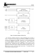
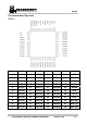
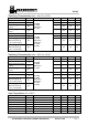
Block Diagram
Figure 1. Functional Schematic of Whole Chip
The schematic of DM163 comprises of several fundamental units as shown in
Figure 1. The grayscale data are input onto the DM163 by the SIN pin and transferred
according to the synchronous clock DCK. Meanwhile, in order to separate the data
into two groups, SELBK is designed as a switch control pin. When a sequence of
data is already transferred onto the chip, the LAT_B=”H” is set to convey it into the
comparator unit. Compared with the counter signals, the grayscale data will
determine the PWM control signal to display varied luminance at driver output. The
Rext resistors are able to set diverse output current levels. The detailed schematic
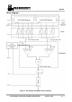
of each channel is shown as Figure 2.