
User Manual

點晶科技股份有限公司
SILICON TOUCH TECHNOLOGY INC. DM163
8x3-CHANNEL CONSTANT CURRENT LED DRIVERS Version: A.004 Page 13
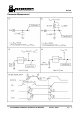
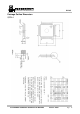
When both 6 bits and 8 bits bank are used for images terms (As shown in Fig. 5), users should set
the controller signal in accordance to the following:
(1) Set SELBK=L (Bank 0) and begin shift in 6 bits correction data
(2) Set SELBK=H (Bank 1) and begin shift in 8 bits image data
(3) Set LAT_B=H to update image data after both 8 bit and 6 bit image data are all inplace.
(4) Repeat steps (1) to (3)
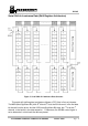
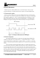
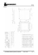
Timing Diagram
Figure 6. Detailed timing diagram of data transference
Figure 6 shows the detailed timing diagram of data transference. The synchronous
clock DCK is designed to trigger at the positive edge. And the LAT_B triggers at the
negative edge. To completely fill up both 6 bit and 8 bit shift register, a total of 336 DCK
count is required (144 DCK for 6bits mode and 192 DCK for 8bits mode). Example
depicted in figure 6 shows 6’b001111 data at 6bits bank and 8’b00001111 at 8bits bank
respectively. Therefore, the average output current is (15/256) x (15/64) x Iout.
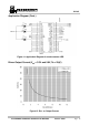
Formula I (out, avg)= (BANK 1/256) x (BANK 0/64) x Iout, provides a useful way to
calculate the input data and the output current. Iout is the reference current value shown
in figure 12. Users could utilize the formula Iout =47*Vrext / Rext to get an approximate
value of Iout.