DM163 Version : A.004 Issue Date : 2005/8/19 File Name : SP-DM163-A.004.doc Total Pages: 21 8x3-CHANNEL CONSTANT CURRENT LED DRIVER 新竹市科學園區展業一路 9 號 7 樓之 1 SILICON TOUCH TECHNOLOGY INC. 9-7F-1, Prosperity Road I, Science Based Industrial Park, Hsin-Chu, Taiwan 300, R.O.C.
點晶科技股份有限公司 DM163 SILICON TOUCH TECHNOLOGY INC. DM163 8x3-CHANNEL CONSTANT CURRENT LED DRIVERS General Description The DM163 is a LED driver that comprises shift registers, data latches, 8x3-channel constant current circuitry with current value set by 3 external resistors, and 64 x 256 gray level PWM (Pulse Width Modulation) function unit. Each channel provides a maximum current of 60 mA. The grayscale data are separated into BANK0 and BANK1 respectively, selected by SELBK pin.
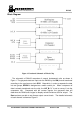
點晶科技股份有限公司 DM163 SILICON TOUCH TECHNOLOGY INC. Block Diagram Figure 1. Functional Schematic of Whole Chip The schematic of DM163 comprises of several fundamental units as shown in Figure 1. The grayscale data are input onto the DM163 by the SIN pin and transferred according to the synchronous clock DCK. Meanwhile, in order to separate the data into two groups, SELBK is designed as a switch control pin.
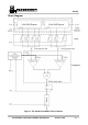
點晶科技股份有限公司 DM163 SILICON TOUCH TECHNOLOGY INC. Block Diagram Figure 2. The Detailed Schematic of Each Channel 8x3-CHANNEL CONSTANT CURRENT LED DRIVERS Version: A.
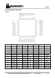
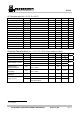
點晶科技股份有限公司 DM163 SILICON TOUCH TECHNOLOGY INC. Pin Connection (Top view) QFP44 Pin No. NAME Pin No. NAME Pin No. NAME Pin No.
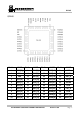
點晶科技股份有限公司 DM163 SILICON TOUCH TECHNOLOGY INC. QFN40 Pin No. NAME Pin No. NAME Pin No. NAME Pin No.
點晶科技股份有限公司 DM163 SILICON TOUCH TECHNOLOGY INC. Pin Description PIN NAME VDDH (R) VDDH (G) VDDH (B) VDD VSS VSS_DR SIN SOUT FUNCTION QFP pin number QFN pin number Output protection pins. 31 28 They could be connected independently 32 29 or to LED supplies (VLED). 33 30 Power supply terminal. 34 31 Ground terminal. 2 3 Driver ground 10, 11, 22, 23 Thermal pad Serial input for grayscale data. 1 2 Serial output for grayscale data. 35 32 Synchronous clock input for serial data 41 38 DCK transfer.
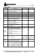
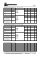
點晶科技股份有限公司 DM163 SILICON TOUCH TECHNOLOGY INC. Maximum Ratings (Ta=25°C, Tj(max) = 140°C) CHARACTERISTIC Supply Voltage Input Voltage Output Current Output Voltage DCK Frequency GCK Frequency GND Terminal Current Power Dissipation Thermal Resistance Operating Temperature Storage Temperature SYMBOL RATING VDD VIN IOUT VOUT FDCK FGCK IGND PD Rth(j-a) Top Tstg UNIT -0.3 ~ 7.0 -0.3 ~ VDD+0.3 60 -0.3 ~ 17 20 20 1440 1.36 ( QFP44); 3.63 (QFN40) (Ta=25°C) 84.42 ( QFP44 ); 31.
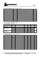
點晶科技股份有限公司 DM163 SILICON TOUCH TECHNOLOGY INC. AC Characteristics (VDD = 3.3 V, Ta = 25°C) CHARACTERISTIC DCK Frequency DCK pulse duration DCK rise/fall time GCK Frequency GCK pulse duration GCK rise/fall time RST_B pulse duration Set-up Time for SIN SYMBOL CONDITION MIN. TYP. MAX.
點晶科技股份有限公司 DM163 SILICON TOUCH TECHNOLOGY INC. Switching Characteristics (VDD = 3.3V, Ta = 25°C) CHARACTERISTIC SOUT Rise time SOUT Fall time SOUT Propagation delay (L to H) SOUT Propagation delay (H to L) IOUT Rise time IOUT Fall time IOUT Propagation delay After GCK or EN_B (L to H / OFF to ON) IOUT Propagation delay After GCK or EN_B (H to L / ON to OFF) SYMBOL MIN. TYP. MAX.
點晶科技股份有限公司 DM163 SILICON TOUCH TECHNOLOGY INC. Parameter Measurement 8x3-CHANNEL CONSTANT CURRENT LED DRIVERS Version: A.
點晶科技股份有限公司 DM163 SILICON TOUCH TECHNOLOGY INC. Serial Shift-In Luminance Data (Shift Register Architecture) Figure 3. Serial Shift-In Luminance Data Structure This serial shift (shift register) architecture follows a FIFO (first-in first-out) formate. The MSB (Most Significant Bit), both 8th bit and 6th bit at the 23rd channel, is the first data bit that shift into the driver. And the LSB (Least Significant Bit) data, the 1st bit at the 1st channel, is the last bit in the data sequence.
點晶科技股份有限公司 DM163 SILICON TOUCH TECHNOLOGY INC. Timing Diagram Figure 4.
點晶科技股份有限公司 DM163 SILICON TOUCH TECHNOLOGY INC. When both 6 bits and 8 bits bank are used for images terms (As shown in Fig. 5), users should set the controller signal in accordance to the following: (1) Set SELBK=L (Bank 0) and begin shift in 6 bits correction data (2) Set SELBK=H (Bank 1) and begin shift in 8 bits image data (3) Set LAT_B=H to update image data after both 8 bit and 6 bit image data are all inplace. (4) Repeat steps (1) to (3) Timing Diagram Figure 6.
點晶科技股份有限公司 DM163 SILICON TOUCH TECHNOLOGY INC. Particular Phenomenon DM163 incorporates a different PWM counter, as described in Figure 2, hence its output waveform demonstrate a very different characteristics compare to conventional PWM counter. (1) Nonconsecutive counter The non-consecutive PWM counter incorporate by DM163 demonstrated a waveform pattern similar to Figure 7. Its waveform is spread-out into each PWM cycle, resulting lots of intermediate pulses during each PWM cycle.
點晶科技股份有限公司 DM163 SILICON TOUCH TECHNOLOGY INC. Application Diagram Figure 10. Application Diagram Note: 1. The RST_B should be connected to controller to initialize the IC. 2. VDDH_R/G/B should be connected to Vled_R/G/B respectively. The Vled_R/G/B are power supply of Red/Green/Blue LEDs. 3. VSS_DR is the ground pin of LEDs. And it could be connected to VSS. 8x3-CHANNEL CONSTANT CURRENT LED DRIVERS Version: A.
點晶科技股份有限公司 DM163 SILICON TOUCH TECHNOLOGY INC. Application Diagram (Cont.) Figure 11. Application Diagram of anode-common LED Driver Output Current (VDD = 3.3V and 5.0V, Ta = 25°C) Figure 12. REXT vs. Output Current 8x3-CHANNEL CONSTANT CURRENT LED DRIVERS Version: A.
點晶科技股份有限公司 DM163 SILICON TOUCH TECHNOLOGY INC. Driver Output Current (Cont.) Figure 13. Vout vs. Output Current The curve shown in Fig 12 is the average result of a large number of samples. Due to chip-to-chip variation in Vrext, users may observe a different Iout-Vout curve than above. However, the curves of VDD=5v and VDD=3.
點晶科技股份有限公司 DM163 SILICON TOUCH TECHNOLOGY INC. Package Outline Dimension QFP44 8x3-CHANNEL CONSTANT CURRENT LED DRIVERS Version: A.
點晶科技股份有限公司 DM163 SILICON TOUCH TECHNOLOGY INC. QFN40 8x3-CHANNEL CONSTANT CURRENT LED DRIVERS Version: A.
點晶科技股份有限公司 DM163 SILICON TOUCH TECHNOLOGY INC. The products listed herein are designed for ordinary electronic applications, such as electrical appliances, audio-visual equipment, communications devices and so on. Hence, it is advisable that the devices should not be used in medical instruments, surgical implants, aerospace machinery, nuclear power control systems, disaster/crime-prevention equipment and the like.