
User Manual

MPU-6000/MPU-6050 Register Map and
Descriptions
Document Number: RM-MPU-6000A-00
Revision: 4.2
Release Date: 08/19/2013
23 of 46
4.12 Registers 49 to 53 – I
2
C Slave 4 Control
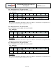
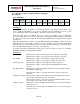
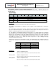
I2C_SLV4_ADDR, I2C_SLV4_REG, I2C_SLV4_DO, I2C_SLV4_CTRL, and I2C_SLV4_DI
Type: Read/Write
Register
(Hex)
Register
(Decimal)
Bit7
Bit6
Bit5
Bit4
Bit3
Bit2
Bit1
Bit0
31
49
I2C_SLV4
_RW
I2C_SLV4_ADDR[6:0]
32
50
I2C_SLV4_REG[7:0]
33
51
I2C_SLV4_DO[7:0]
34
52
I2C_SLV4_
EN
I2C_SLV4
_INT_EN
I2C_SLV4
_REG_DIS
I2C_MST_DLY[4:0]
35
53
I2C_SLV4_DI[7:0]
Description:
These registers describe the data transfer sequence for Slave 4. The characteristics of Slave 4 differ
greatly from those of Slaves 0-3. For further information regarding the characteristics of Slaves 0-3,
please refer to Registers 37 to 48.
I
2
C slave data transactions between the MPU-60X0 and Slave 4 are set as either read or write
operations by the I2C_SLV4_RW bit. When this bit is 1, the transfer is a read operation. When the bit
is 0, the transfer is a write operation.
I2C_SLV4_ADDR is used to specify the I
2
C slave address of Slave 4.
Data transfer starts at an internal register within Slave 4. This register address is specified by
I2C_SLV4_REG.
In read mode, the result of the read will be available in I2C_SLV4_DI. In write mode, the contents of
I2C_SLV4_DO will be written into the slave device.
A data transaction is performed only if the I2C_SLV4_EN bit is set to 1. The data transaction should
be enabled once its parameters are configured in the _ADDR and _REG registers. For write, the
_DO register is also required. I2C_SLV4_EN will be cleared after the transaction is performed once.
An interrupt is triggered at the completion of a Slave 4 data transaction if the interrupt is enabled .
The status of this interrupt can be observed in Register 54.
When I2C_SLV4_REG_DIS is set to 1, the transaction will read or write data instead of writing a
register address. This bit should equal 0 when specifying the register address within the Slave
device to/from which the ensuing data transaction will take place.
I2C_MST_DLY configures the reduced access rate of I
2
C slaves relative to the Sample Rate. When
a slave’s access rate is decreased relative to the Sample Rate, the slave is accessed every
1 / (1 + I2C_MST_DLY) samples
This base Sample Rate in turn is determined by SMPLRT_DIV (register 25) and DLPF_CFG
(register 26). Whether a slave’s access rate is reduced relative to the Sample Rate is determined by
I2C_MST_DELAY_CTRL (register 103).
For further information regarding the Sample Rate, please refer to register 25.
Slave 4 transactions are performed after Slave 0, 1, 2 and 3 transactions have been completed.
Thus the maximum rate for Slave 4 transactions is determined by the Sample Rate as defined in
Register 25.