
User Manual

MPU-6000/MPU-6050 Register Map and
Descriptions
Document Number: RM-MPU-6000A-00
Revision: 4.2
Release Date: 08/19/2013
22 of 46
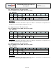
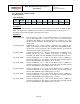
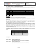
4.9 Registers 40 to 42 – I
2
C Slave 1 Control
I2C_SLV1_ADDR, I2C_SLV1_REG, and I2C_SLV1_CTRL
Type: Read/Write
Register
(Hex)
Register
(Decimal)
Bit7
Bit6
Bit5
Bit4
Bit3
Bit2
Bit1
Bit0
28
40
I2C_SLV1
_RW
I2C_SLV1_ADDR[6:0]
29
41
I2C_SLV1_REG[7:0]
2A
42
I2C_SLV1
_EN
I2C_SLV1
_BYTE
_SW
I2C_SLV1_
REG_DIS
I2C_SLV
1_GRP
I2C_SLV1_LEN[3:0]
Description:
These registers describe the data transfer sequence for Slave 1. Their functions correspond to those
described for the Slave 0 registers (Registers 37 to 39).
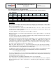
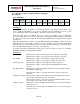
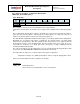
4.10 Registers 43 to 45 – I
2
C Slave 2 Control
I2C_SLV2_ADDR, I2C_SLV2_REG, and I2C_SLV2_CTRL
Type: Read/Write
Register
(Hex)
Register
(Decimal)
Bit7
Bit6
Bit5
Bit4
Bit3
Bit2
Bit1
Bit0
2B
43
I2C_SLV2
_RW
I2C_SLV2_ADDR[6:0]
2C
44
I2C_SLV2_REG[7:0]
2D
45
I2C_SLV2
_EN
I2C_SLV2
_BYTE
_SW
I2C_SLV2_
REG_DIS
I2C_SLV
2_GRP
I2C_SLV2_LEN[3:0]
Description:
These registers describe the data transfer sequence for Slave 2. Their functions correspond to those
described for the Slave 0 registers (Registers 37 to 39).
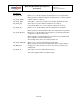
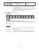
4.11 Registers 46 to 48 – I
2
C Slave 3 Control
I2C_SLV3_ADDR, I2C_SLV3_REG, and I2C_SLV3_CTRL
Type: Read/Write
Register
(Hex)
Register
(Decimal)
Bit7
Bit6
Bit5
Bit4
Bit3
Bit2
Bit1
Bit0
2E
46
I2C_SLV3
_RW
I2C_SLV3_ADDR[6:0]
2F
47
I2C_SLV3_REG[7:0]
30
48
I2C_SLV3
_EN
I2C_SLV3
_BYTE
_SW
I2C_SLV3_
REG_DIS
I2C_SLV
3_GRP
I2C_SLV3_LEN[3:0]
Description:
These registers describe the data transfer sequence for Slave 3. Their functions correspond to those
described for the Slave 0 registers (Registers 37 to 39).