
User Manual

MPU-6000/MPU-6050 Register Map and
Descriptions
Document Number: RM-MPU-6000A-00
Revision: 4.2
Release Date: 08/19/2013
21 of 46
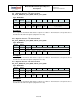
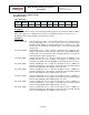
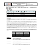
Byte Swapping Example
The following example demonstrates byte swapping for I2C_SLV0_BYTE_SW = 1,
I2C_SLV0_GRP = 0, I2C_SLV0_REG = 0x01, and I2C_SLV0_LEN = 0x4:
1. The first byte, read from Slave 0 register 0x01, will be stored at EXT_SENS_DATA_00. Because
I2C_SLV0_GRP = 0, bytes from even, then odd register addresses will be paired together as
word pairs. Since the read operation started from an odd register address instead of an even
address, only one byte is read.
2. The second and third bytes will be swapped, since I2C_SLV0_BYTE_SW = 1 and
I2C_SLV0_REG[0] = 1. The data read from 0x02 will be stored at EXT_SENS_DATA_02, and
the data read from 0x03 will be stored at EXT_SENS_DATA_01.
3. The last byte, read from address 0x04, will be stored at EXT_SENS_DATA_03. Because there is
only one byte remaining in the read operation, byte swapping will not occur.
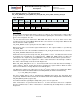
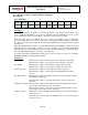
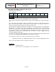
Slave Access Example
Slave 0 is accessed at the Sample Rate, while Slave 1 is accessed at half the Sample Rate. The
other slaves are disabled. In the first cycle, both Slave 0 and Slave 1 will be accessed. However, in
the second cycle, only Slave 0 will be accessed. In the third cycle, both Slave 0 and Slave 1 will be
accessed. In the fourth cycle, only Slave 0 will be accessed. This pattern continues.