
User Manual

MPU-6000/MPU-6050 Register Map and
Descriptions
Document Number: RM-MPU-6000A-00
Revision: 4.2
Release Date: 08/19/2013
19 of 46
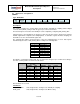
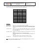
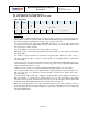
4.8 Registers 37 to 39 – I
2
C Slave 0 Control
I2C_SLV0_ADDR, I2C_SLV0_REG, and I2C_SLV0_CTRL
Type: Read/Write
Register
(Hex)
Register
(Decimal)
Bit7
Bit6
Bit5
Bit4
Bit3
Bit2
Bit1
Bit0
25
37
I2C_SLV0
_RW
I2C_SLV0_ADDR[6:0]
26
38
I2C_SLV0_REG[7:0]
27
39
I2C_SLV0
_EN
I2C_SLV0
_BYTE
_SW
I2C_SLV0_
REG_DIS
I2C_SLV
0_GRP
I2C_SLV0_LEN[3:0]
Description:
These registers configure the data transfer sequence for Slave 0. Slaves 1, 2, and 3 also behave in a
similar manner to Slave 0. However, Slave 4’s characteristics differ greatly from those of Slaves 0-3.
For further information regarding Slave 4, please refer to registers 49 to 53.
I
2
C slave data transactions between the MPU-60X0 and Slave 0 are set as either read or write
operations by the I2C_SLV0_RW bit. When this bit is 1, the transfer is a read operation. When the bit
is 0, the transfer is a write operation.
I2C_SLV0_ADDR is used to specify the I
2
C slave address of Slave 0.
Data transfer starts at an internal register within Slave 0. This address of this register is specified by
I2C_SLV0_REG.
The number of bytes transferred is specified by I2C_SLV0_LEN. When more than 1 byte is
transferred (I2C_SLV0_LEN > 1), data is read from (written to) sequential addresses starting from
I2C_SLV0_REG.
In read mode, the result of the read is placed in the lowest available EXT_SENS_DATA register. For
further information regarding the allocation of read results, please refer to the EXT_SENS_DATA
register description (Registers 73 – 96).
In write mode, the contents of I2C_SLV0_DO (Register 99) will be written to the slave device.
I2C_SLV0_EN enables Slave 0 for I
2
C data transaction. A data transaction is performed only if more
than zero bytes are to be transferred (I2C_SLV0_LEN > 0) between an enabled slave device
(I2C_SLV0_EN = 1).
I2C_SLV0_BYTE_SW configures byte swapping of word pairs. When byte swapping is enabled, the
high and low bytes of a word pair are swapped. Please refer to I2C_SLV0_GRP for the pairing
convention of the word pairs. When this bit is cleared to 0, bytes transferred to and from Slave 0 will
be written to EXT_SENS_DATA registers in the order they were transferred.
When I2C_SLV0_REG_DIS is set to 1, the transaction will read or write data only. When cleared to
0, the transaction will write a register address prior to reading or writing data. This bit should equal 0
when specifying the register address within the Slave device to/from which the ensuing data
transaction will take place.