InvenSense Inc. 1197 Borregas Ave, Sunnyvale, CA 94089 U.S.A. Tel: +1 (408) 988-7339 Fax: +1 (408) 988-8104 Website: www.invensense.com Document Number: RM-MPU-6000A-00 Revision: 4.2 Release Date: 08/19/2013 MPU-6000 and MPU-6050 Register Map and Descriptions Revision 4.
MPU-6000/MPU-6050 Register Map and Descriptions Document Number: RM-MPU-6000A-00 Revision: 4.2 Release Date: 08/19/2013 CONTENTS 1 REVISION HISTORY ...................................................................................................................................4 2 PURPOSE AND SCOPE .............................................................................................................................5 3 REGISTER MAP ..............................................................
MPU-6000/MPU-6050 Register Map and Descriptions Document Number: RM-MPU-6000A-00 Revision: 4.2 Release Date: 08/19/2013 4.30 REGISTER 114 AND 115 – FIFO COUNT REGISTERS ...........................................................................43 4.31 REGISTER 116 – FIFO READ W RITE ..................................................................................................44 4.32 REGISTER 117 – W HO AM I...........................................................................................
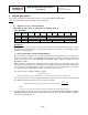
MPU-6000/MPU-6050 Register Map and Descriptions 1 Document Number: RM-MPU-6000A-00 Revision: 4.2 Release Date: 08/19/2013 Revision History Revision Date Revision Description 11/29/2010 1.0 Initial Release 04/20/2011 1.1 Updated register map and descriptions to reflect enhanced register functionality. 05/19/2011 2.0 10/07/2011 3.0 10/24/2011 3.1 Updates for Rev C silicon: Edits for readability (section 2.1) Edits for changes in functionality (section 3, 4.4, 4.6, 4.7, 4.8, 4.21, 4.22, 4.
MPU-6000/MPU-6050 Register Map and Descriptions 2 Document Number: RM-MPU-6000A-00 Revision: 4.2 Release Date: 08/19/2013 Purpose and Scope This document provides preliminary information regarding the register map and descriptions for the Motion Processing Units™ MPU-6000™ and MPU-6050™, collectively called the MPU-60X0™ or MPU™.
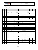
MPU-6000/MPU-6050 Register Map and Descriptions 3 Document Number: RM-MPU-6000A-00 Revision: 4.2 Release Date: 08/19/2013 Register Map The register map for the MPU-60X0 is listed below. Addr (Hex) Addr (Dec.
MPU-6000/MPU-6050 Register Map and Descriptions Document Number: RM-MPU-6000A-00 Revision: 4.2 Release Date: 08/19/2013 Addr (Hex) Addr (Dec.
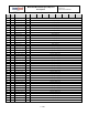
MPU-6000/MPU-6050 Register Map and Descriptions Addr (Hex) Addr (Dec.) Register Name Serial I/F 67 103 I2C_MST_DELAY_CT RL 68 104 6A Document Number: RM-MPU-6000A-00 Revision: 4.
Document Number: RM-MPU-6000A-00 Revision: 4.2 Release Date: 08/19/2013 MPU-6000/MPU-6050 Register Map and Descriptions 4 Register Descriptions This section describes the function and contents of each register within the MPU-60X0. Note: The device will come up in sleep mode upon power-up. 4.
MPU-6000/MPU-6050 Register Map and Descriptions Document Number: RM-MPU-6000A-00 Revision: 4.2 Release Date: 08/19/2013 Obtaining the Gyroscope Factory Trim (FT) Value If InvenSense MotionApps software is not used, the procedure detailed below should be followed to obtain the Factory trim value of the self test response (FT) mentioned above. For the specific registers mentioned below, please refer to registers 13-15. The Factory trim value of the self test response (FT) is calculated as shown below.
MPU-6000/MPU-6050 Register Map and Descriptions Document Number: RM-MPU-6000A-00 Revision: 4.2 Release Date: 08/19/2013 Obtaining the Accelerometer Factory Trim (FT) Value If InvenSense MotionApps software is not used, the procedure detailed below should be followed to obtain the Factory trim value of the self test response (FT) mentioned above. For the specific registers mentioned below, please refer to registers 13-16. The Factory trim value of the self test response (FT) is calculated as shown below.
MPU-6000/MPU-6050 Register Map and Descriptions Document Number: RM-MPU-6000A-00 Revision: 4.2 Release Date: 08/19/2013 This register specifies the divider from the gyroscope output rate used to generate the Sample Rate for the MPU-60X0. The sensor register output, FIFO output, and DMP sampling are all based on the Sample Rate.
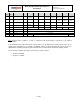
MPU-6000/MPU-6050 Register Map and Descriptions Document Number: RM-MPU-6000A-00 Revision: 4.2 Release Date: 08/19/2013 4.3 Register 26 – Configuration CONFIG Type: Read/Write Register (Hex) Register (Decimal) Bit7 Bit6 1A 26 - - Bit5 Bit4 Bit3 EXT_SYNC_SET[2:0] Bit2 Bit1 Bit0 DLPF_CFG[2:0] Description: This register configures the external Frame Synchronization (FSYNC) pin sampling and the Digital Low Pass Filter (DLPF) setting for both the gyroscopes and accelerometers.
MPU-6000/MPU-6050 Register Map and Descriptions Document Number: RM-MPU-6000A-00 Revision: 4.2 Release Date: 08/19/2013 4.4 Register 27 – Gyroscope Configuration GYRO_CONFIG Type: Read/Write Register (Hex) Register (Decimal) Bit7 Bit6 Bit5 1B 27 XG_ST YG_ST ZG_ST Bit4 Bit3 FS_SEL[1:0] Bit2 Bit1 Bit0 - - - Description: This register is used to trigger gyroscope self-test and configure the gyroscopes’ full scale range.
MPU-6000/MPU-6050 Register Map and Descriptions Document Number: RM-MPU-6000A-00 Revision: 4.2 Release Date: 08/19/2013 4.5 Register 28 – Accelerometer Configuration ACCEL_CONFIG Type: Read/Write Register (Hex) Register (Decimal) Bit7 Bit6 Bit5 1C 28 XA_ST YA_ST ZA_ST Bit4 Bit3 AFS_SEL[1:0] Bit2 Bit1 Bit0 - Description: This register is used to trigger accelerometer self test and configure the accelerometer full scale range.
MPU-6000/MPU-6050 Register Map and Descriptions Document Number: RM-MPU-6000A-00 Revision: 4.2 Release Date: 08/19/2013 Parameters: XA_ST When set to 1, the X- Axis accelerometer performs self test. YA_ST When set to 1, the Y- Axis accelerometer performs self test. ZA_ST When set to 1, the Z- Axis accelerometer performs self test. AFS_SEL 2-bit unsigned value. Selects the full scale range of accelerometers. 4.
Document Number: RM-MPU-6000A-00 Revision: 4.2 Release Date: 08/19/2013 MPU-6000/MPU-6050 Register Map and Descriptions SLV2_ FIFO_EN When set to 1, this bit enables EXT_SENS_DATA registers (Registers 73 to 96) associated with Slave 2 to be written into the FIFO buffer. SLV1_ FIFO_EN When set to 1, this bit enables EXT_SENS_DATA registers (Registers 73 to 96) associated with Slave 1 to be written into the FIFO buffer.
MPU-6000/MPU-6050 Register Map and Descriptions Document Number: RM-MPU-6000A-00 Revision: 4.2 Release Date: 08/19/2013 I2C_MST_CLK is a 4 bit unsigned value which configures a divider on the MPU-60X0 internal 8MHz 2 clock.
MPU-6000/MPU-6050 Register Map and Descriptions Document Number: RM-MPU-6000A-00 Revision: 4.2 Release Date: 08/19/2013 2 4.
MPU-6000/MPU-6050 Register Map and Descriptions Document Number: RM-MPU-6000A-00 Revision: 4.2 Release Date: 08/19/2013 I2C_SLV0_GRP specifies the grouping order of word pairs received from registers. When cleared to 0, bytes from register addresses 0 and 1, 2 and 3, etc (even, then odd register addresses) are paired to form a word. When set to 1, bytes from register addresses are paired 1 and 2, 3 and 4, etc. (odd, then even register addresses) are paired to form a word.
MPU-6000/MPU-6050 Register Map and Descriptions Document Number: RM-MPU-6000A-00 Revision: 4.2 Release Date: 08/19/2013 Byte Swapping Example The following example demonstrates byte swapping for I2C_SLV0_BYTE_SW I2C_SLV0_GRP = 0, I2C_SLV0_REG = 0x01, and I2C_SLV0_LEN = 0x4: = 1, 1. The first byte, read from Slave 0 register 0x01, will be stored at EXT_SENS_DATA_00. Because I2C_SLV0_GRP = 0, bytes from even, then odd register addresses will be paired together as word pairs.
MPU-6000/MPU-6050 Register Map and Descriptions Document Number: RM-MPU-6000A-00 Revision: 4.2 Release Date: 08/19/2013 2 4.
MPU-6000/MPU-6050 Register Map and Descriptions Document Number: RM-MPU-6000A-00 Revision: 4.2 Release Date: 08/19/2013 2 4.
MPU-6000/MPU-6050 Register Map and Descriptions Document Number: RM-MPU-6000A-00 Revision: 4.2 Release Date: 08/19/2013 Parameters: I2C_SLV4_RW When set to 1, this bit configures the data transfer as a read operation. When cleared to 0, this bit configures the data transfer as a write operation. I2C_SLV4_ADDR 7-bit I C address for Slave 4. I2C_SLV4_REG 8-bit address of the Slave 4 register to/from which data transfer starts. I2C_SLV4_DO This register stores the data to be written into the Slave 4.
Document Number: RM-MPU-6000A-00 Revision: 4.2 Release Date: 08/19/2013 MPU-6000/MPU-6050 Register Map and Descriptions 2 4.
MPU-6000/MPU-6050 Register Map and Descriptions Document Number: RM-MPU-6000A-00 Revision: 4.2 Release Date: 08/19/2013 4.14 Register 55 – INT Pin / Bypass Enable Configuration INT_PIN_CFG Type: Read/Write Register (Hex) Register (Decimal) Bit7 Bit6 Bit5 Bit4 Bit3 Bit2 Bit1 Bit0 37 55 INT_LEVEL INT_OPEN LATCH _INT_EN INT_RD _CLEAR FSYNC_ INT_LEVEL FSYNC_ INT_EN I2C _BYPASS _EN - Description: This register configures the behavior of the interrupt signals at the INT pins.
MPU-6000/MPU-6050 Register Map and Descriptions I2C_BYPASS_EN Document Number: RM-MPU-6000A-00 Revision: 4.2 Release Date: 08/19/2013 When this bit is equal to 1 and I2C_MST_EN (Register 106 bit[5]) is equal to 0, the host application processor will be able to directly access the auxiliary 2 I C bus of the MPU-60X0.
MPU-6000/MPU-6050 Register Map and Descriptions Document Number: RM-MPU-6000A-00 Revision: 4.2 Release Date: 08/19/2013 4.16 Register 58 – Interrupt Status INT_STATUS Type: Read Only Register (Hex) Register (Decimal) Bit7 Bit6 Bit5 Bit4 Bit3 Bit2 Bit1 Bit0 3A 58 - - - FIFO _OFLOW _INT I2C_MST _INT - - DATA _RDY_INT Description: This register shows the interrupt status of each interrupt generation source. Each bit will clear after the register is read.
MPU-6000/MPU-6050 Register Map and Descriptions Document Number: RM-MPU-6000A-00 Revision: 4.2 Release Date: 08/19/2013 4.
MPU-6000/MPU-6050 Register Map and Descriptions Document Number: RM-MPU-6000A-00 Revision: 4.2 Release Date: 08/19/2013 4.18 Registers 65 and 66 – Temperature Measurement TEMP_OUT_H and TEMP_OUT_L Type: Read Only Register (Hex) Register (Decimal) 41 65 TEMP_OUT[15:8] 42 66 TEMP_OUT[7:0] Bit7 Bit6 Bit5 Bit4 Bit3 Bit2 Bit1 Bit0 Description: These registers store the most recent temperature sensor measurement.
MPU-6000/MPU-6050 Register Map and Descriptions Document Number: RM-MPU-6000A-00 Revision: 4.2 Release Date: 08/19/2013 4.
MPU-6000/MPU-6050 Register Map and Descriptions Document Number: RM-MPU-6000A-00 Revision: 4.2 Release Date: 08/19/2013 4.
MPU-6000/MPU-6050 Register Map and Descriptions Document Number: RM-MPU-6000A-00 Revision: 4.2 Release Date: 08/19/2013 Each enabled slave will have EXT_SENS_DATA registers associated with it by number of bytes read (I2C_SLVx_LEN) in order of slave number, starting from EXT_SENS_DATA_00. Note that this means enabling or disabling a slave may change the higher numbered slaves’ associated registers.
MPU-6000/MPU-6050 Register Map and Descriptions Document Number: RM-MPU-6000A-00 Revision: 4.2 Release Date: 08/19/2013 2 4.21 Register 99 – I C Slave 0 Data Out I2C_SLV0_DO Type: Read/Write Register (Hex) Register (Decimal) 63 99 Bit7 Bit6 Bit5 Bit4 Bit3 Bit2 Bit1 Bit0 I2C_SLV0_DO[7:0] Description: This register holds the output data written into Slave 0 when Slave 0 is set to write mode. For further information regarding Slave 0 control, please refer to Registers 37 to 39.
MPU-6000/MPU-6050 Register Map and Descriptions Document Number: RM-MPU-6000A-00 Revision: 4.2 Release Date: 08/19/2013 2 4.23 Register 101 – I C Slave 2 Data Out I2C_SLV2_DO Type: Read/Write Register (Hex) Register (Decimal) 65 101 Bit7 Bit6 Bit5 Bit4 Bit3 Bit2 Bit1 Bit0 I2C_SLV2_DO[7:0] Description: This register holds the output data written into Slave 2 when Slave 2 is set to write mode. For further information regarding Slave 2 control, please refer to Registers 43 to 45.
MPU-6000/MPU-6050 Register Map and Descriptions Document Number: RM-MPU-6000A-00 Revision: 4.2 Release Date: 08/19/2013 2 4.25 Register 103 – I C Master Delay Control I2C_MST_DELAY_CTRL Type: Read/Write Register (Hex) Register (Decimal) Bit7 Bit6 Bit5 Bit4 Bit3 Bit2 Bit1 Bit0 103 DELAY _ES _SHADOW - - I2C_SLV4 _DLY_EN I2C_SLV3 _DLY_EN I2C_SLV2 _DLY_EN I2C_SLV1 _DLY_EN I2C_SLV0 _DLY_EN 67 Description: This register is used to specify the timing of external sensor data shadowing.
Document Number: RM-MPU-6000A-00 Revision: 4.2 Release Date: 08/19/2013 MPU-6000/MPU-6050 Register Map and Descriptions 4.26 Register 104 – Signal Path Reset SIGNAL_PATH_RESET Type: Write Only Register (Hex) Register (Decimal) 68 Bit7 104 - Bit6 - Bit5 - Bit4 - Bit3 Bit2 Bit1 Bit0 - GYRO _RESET ACCEL _RESET TEMP _RESET Description: This register is used to reset the analog and digital signal paths of the gyroscope, accelerometer, and temperature sensors.
Document Number: RM-MPU-6000A-00 Revision: 4.2 Release Date: 08/19/2013 MPU-6000/MPU-6050 Register Map and Descriptions 4.27 Register 106 – User Control USER_CTRL Type: Read/Write Register (Hex) Register (Decimal) Bit7 Bit6 Bit5 Bit4 Bit3 Bit2 Bit1 Bit0 6A 106 - FIFO_EN I2C_MST _EN I2C_IF _DIS - FIFO _RESET I2C_MST _RESET SIG_COND _RESET Description: 2 This register allows the user to enable and disable the FIFO buffer, I C Master Mode, and primary 2 2 I C interface.
MPU-6000/MPU-6050 Register Map and Descriptions SIG_COND_RESET Document Number: RM-MPU-6000A-00 Revision: 4.2 Release Date: 08/19/2013 When set to 1, this bit resets the signal paths for all sensors (gyroscopes, accelerometers, and temperature sensor). This operation will also clear the sensor registers. This bit automatically clears to 0 after the reset has been triggered. When resetting only the signal path (and not the sensor registers), please use Register 104, SIGNAL_PATH_RESET.
MPU-6000/MPU-6050 Register Map and Descriptions Document Number: RM-MPU-6000A-00 Revision: 4.2 Release Date: 08/19/2013 4.28 Register 107 – Power Management 1 PWR_MGMT_1 Type: Read/Write Register (Hex) Register (Decimal) Bit7 Bit6 Bit5 Bit4 Bit3 6B 107 DEVICE _RESET SLEEP CYCLE - TEMP_DIS Bit2 Bit1 Bit0 CLKSEL[2:0] Description: This register allows the user to configure the power mode and clock source.
MPU-6000/MPU-6050 Register Map and Descriptions Document Number: RM-MPU-6000A-00 Revision: 4.2 Release Date: 08/19/2013 Parameters: DEVICE_RESET When set to 1, this bit resets all internal registers to their default values. The bit automatically clears to 0 once the reset is done. The default values for each register can be found in Section 3. SLEEP When set to 1, this bit puts the MPU-60X0 into sleep mode.
MPU-6000/MPU-6050 Register Map and Descriptions Document Number: RM-MPU-6000A-00 Revision: 4.2 Release Date: 08/19/2013 4.29 Register 108 – Power Management 2 PWR_MGMT_2 Type: Read/Write Register (Hex) Register (Decimal) 6C 108 Bit7 Bit6 LP_WAKE_CTRL[1:0] Bit5 Bit4 Bit3 Bit2 Bit1 Bit0 STBY_XA STBY_YA STBY_ZA STBY_XG STBY_YG STBY_ZG Description: This register allows the user to configure the frequency of wake-ups in Accelerometer Only Low Power Mode.
MPU-6000/MPU-6050 Register Map and Descriptions Document Number: RM-MPU-6000A-00 Revision: 4.2 Release Date: 08/19/2013 4.30 Register 114 and 115 – FIFO Count Registers FIFO_COUNT_H and FIFO_COUNT_L Type: Read Only Register (Hex) Register (Decimal) 72 114 FIFO_COUNT[15:8] 73 115 FIFO_COUNT[7:0] Bit7 Bit6 Bit5 Bit4 Bit3 Bit2 Bit1 Bit0 Description: These registers keep track of the number of samples currently in the FIFO buffer. These registers shadow the FIFO Count value.
MPU-6000/MPU-6050 Register Map and Descriptions Document Number: RM-MPU-6000A-00 Revision: 4.2 Release Date: 08/19/2013 4.31 Register 116 – FIFO Read Write FIFO_R_W Type: Read/Write Register (Hex) Register (Decimal) 74 116 Bit7 Bit6 Bit5 Bit4 Bit3 Bit2 Bit1 Bit0 FIFO_DATA[7:0] Description: This register is used to read and write data from the FIFO buffer. Data is written to the FIFO in order of register number (from lowest to highest).
MPU-6000/MPU-6050 Register Map and Descriptions Document Number: RM-MPU-6000A-00 Revision: 4.2 Release Date: 08/19/2013 4.32 Register 117 – Who Am I WHO_AM_I Type: Read Only Register (Hex) Register (Decimal) Bit7 75 117 - Bit6 Bit5 Bit4 Bit3 WHO_AM_I[6:1] Bit2 Bit1 Bit0 - Description: This register is used to verify the identity of the device. The contents of WHO_AM_I are the upper 6 2 2 bits of the MPU-60X0’s 7-bit I C address.
MPU-6000/MPU-6050 Register Map and Descriptions Document Number: RM-MPU-6000A-00 Revision: 4.2 Release Date: 08/19/2013 This information furnished by InvenSense is believed to be accurate and reliable. However, no responsibility is assumed by InvenSense for its use, or for any infringements of patents or other rights of third parties that may result from its use. Specifications are subject to change without notice.