
User's Manual


Innovator CU0TD-1/CU0RD-1 – CU4TD/CU4RD ATSC Board Descriptions
Transmitter/Regenerative Translator
Instruction Manual, Rev. 2 110
The Input Fault is generated by comparator U7C and presets the PIN attenuator and ALC
circuit to maximum attenuation whenever the input signal drops below about -7 dBm.
Test point TP2 allows the user to measure the detected input voltage.
The VSWR cutback circuit is set so that the ALC circuit will start reducing RF drive once
the Reflected power reaches a level of about 6% and will keep reducing the drive to
maintain that level. The cutback is generated by U8A, U8B and their associated
components that diode-or the metering voltages. The forward power is scaled to 2V =
100 % and the reflected power is scaled to 2V = 25%. The Reflected metering voltage
is doubled again by U8B so that when the voltage of U8B exceeds the voltage at the
output of U8A, the reflected power takes over the ALC circuit. Once the U8B voltage
drops below the forward power at U8A, the forward power takes over again.
The VSWR shutdown circuit will shut the drawer down if the Reflected power increases to
15% or higher, which can happen if the drawer sees reflected power when the ALC is in
manual.
The Overdrive protection looks at a sample of the RF signal that is applied to J1 of the
board. The peak level of this signal is detected and can be measured on TP1. This
voltage is applied to a comparator with the threshold set by R38. If this threshold is
exceeded, the ALC circuit mutes then ramps up to try again. This circuit also works in
manual gain as well.
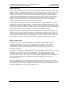
(A6) Amplifier Assembly
Heatsink
Temperature
Sensor
RF Input
+10 dBm
RF Output
+46 dBm
+32 dBm
Figure 61: Typical Amplifier Assembly Block Diagram
NOTE: There are a number of different (A6) Amplifier Assemblies used in the multiple
CX transmitter and driver drawers. They are listed in the following sections. Use the
assembly that applies to your particular driver or transmitter or translator.