
User's Manual


Innovator CU0TD-1/CU0RD-1 – CU4TD/CU4RD ATSC Board Descriptions
Transmitter/Regenerative Translator
Instruction Manual, Rev. 2 109
NOTES: SW1-8 operation is available in software versions greater than or equal to 2.3
with hardware versions greater than or equal to D0, unless the board was factory
modified. These switch positions are factory set for your system and should not be
changed.
(A5) ALC Board, Innovator CX Series(1315006)
Pin AttenuatorJ1
RF Input
Input Loss
Detector
Auto/Man Select
ALC
TP4
Mute from
Control Circuit
J2
RF Output
TP1
Overdrive Detect
Output Power
Reflected Power
Input Power
Reference
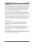
Figure 60: ALC Board Block Diagram
The ALC Board, Innovator CX Series, is used to control the RF drive power to the RF
amplifier chain in the CU0TD/RD-1 thru CU0TD/RD-5 systems. The board accepts an 8-
VSB RF input signal at a nominal input level of -3 dBm average power and amplifies it to
whatever drive level is necessary to drive the final RF amplifier in the drawer to full
power. The input signal to the board at J1 is split by U4, with one half of the signal
driving a PIN diode attenuator, DS1 and DS2, and the other half driving a detector, U13,
that is used to mute the PIN attenuator when there is no input signal. The output of the
PIN attenuator is sent to two cascaded amplifiers, U2 and U3, which are capable of
generating +10 dBm average power from the board at J2.
The PIN attenuator is driven by an ALC circuit or by a manual fixed voltage bias,
depending on the position of switch S1. When the switch is pointing to the left, looking
from the front of the drawer, the ALC circuit is enabled. When the switch is pointing to
the right, the ALC circuit is disabled and the PIN attenuator is controlled through the
Manual gain pot R62. When the switch is in either ALC or manual, the voltage in the
unused circuit is preset low by the circuitry connected to pins 4-6 on SW1. This allows
the RF power to ramp up slowly to full power when the switch changes positions. CR8,
C33 and associated components control the ramp up speed of the manual gain circuit.
CR9, C42 and their associated circuits do the same thing for the ALC circuit. The
practical effect of this is to preset the RF drive power to near zero output power when
enabling and disabling the ALC, followed by a slow controlled ramp up of power.
The ALC circuit normally attempts to hold the drawer output power constant, but there
are four faults that can override this. These faults are Input Fault, VSWR Cutback Fault,
VSWR Shutdown Fault and Overdrive Fault.