
Manual Chapter 3


500-Watt UHF Transmitter Chapter 3, Circuit Descriptions
425A, Rev. 0 3-25
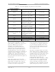
Table 3-1. 600-Watt Amplifier Tray Boards and Assemblies
MAJOR ASSEMBLY
DESIGNATOR
BOARD/ASSEMBLY NAME DRAWING NUMBER
A1-A1
Phase shifter board
(mounted in [A1] an RF
enclosure assembly)
1198-1602
A2-A1
Filter/amplifier board
(mounted in [A2] an RF
enclosure assembly)
1218-1104
A2-A2
High band driver board
(mounted in [A2] an RF
enclosure assembly)
1219-1103
A3-A1
Overdrive protection board
(mounted in [A3] an RF
enclosure assembly)
1198-1601
A3-A2
High band VHF amplifier
board (mounted in [A3] an
RF enclosure assembly)
1219-1114
A3-A3
4-way splitter board
(mounted in [A3] an RF
enclosure assembly)
1219-1101
A4-A1, A4-A2, A4-A3, and
A4-A4
Four high band VHF
amplifier boards (mounted
in [A4] an RF enclosure
assembly)
1218-1201
A5-A1 4-way combiner board 1219-1102
A13 AGC control board 1142-1601
A8 Current metering board 1198-1609
A10
+48 VDC switching power
supply assembly
The on-channel visual RF or aural RF
input signal (+3 dBm) enters the rear of
the tray at BNC jack J1 and is fed
through J1 of the (A1) enclosure
assembly to J1 of (A1-A1) the phase
shifter board (1198-1602). The board
provides a phase shifter adjustment of
the RF signal that is needed to provide
maximum output during the combining of
multiple 600-watt amplifier trays in an
amplifier array. Front panel-mounted
phase shift potentiometer R2 connects to
J3 on the board and controls the phase of
the RF signal.
If the input signal level to the phase
shifter board falls below a preset level, a
high, which is an input fault, connects
from J5 of the board to J14 on the AGC
control board. When an input fault
occurs, the AGC control board generates
a fault output at J1, which is connected
to J4 on the filter/amplifier board. The
fault cuts back the RF signal level using
the pin-diode attenuator circuit on the
filter/amplifier board.
The phase-controlled output at J2 of the
phase shifter board (+2 dBm) is directed
to J7, the input jack of (A2-A1) the filter
amplifier board (1218-1104) that is made
up of two circuits. The first circuit is a
channel filter that is adjusted for the
desired channel frequency and
bandwidth. The filtered output (+1 dBm)
is connected to the second circuit; this
circuit contains two amplifiers. The RF
connects through a pin-diode circuit to
amplifier IC U1. The amplitude of the RF
signal through the pin-diode attenuator