
User Guide
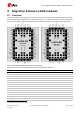
Table Of Contents
- Document information
- Contents
- 1 LARA-R2 / LARA-R6 modules description
- 2 Migration between LARA modules
- 2.1 Overview
- 2.2 Pin-out comparison between LARA modules
- 2.3 Interfaces comparison between LARA modules
- 2.3.1 VCC module supply input
- 2.3.2 V_INT 1.8 V supply output
- 2.3.3 V_BCKP RTC supply input/output
- 2.3.4 Cellular RF interfaces
- 2.3.5 System control interfaces
- 2.3.6 SIM interface
- 2.3.7 UART interfaces
- 2.3.8 USB interface
- 2.3.9 I2C interface
- 2.3.10 Digital audio interface
- 2.3.11 Clock output
- 2.3.12 GPIOs
- 2.3.13 Antenna dynamic tuning
- 2.3.14 Reserved pins
- 2.3.15 Other considerations and test points
- 2.4 Schematic for LARA modules integration
- Appendix
- A Glossary
- Related documents
- Revision history
- Contact

LARA-R2/R6 migration guide - Application note
UBX-21010015 - R02 Contents Page 3 of 25
C1-Public
Contents
Document information ................................................................................................................................ 2
Contents .......................................................................................................................................................... 3
1 LARA-R2 / LARA-R6 modules description .................................................................................... 4
2 Migration between LARA modules .................................................................................................. 7
2.1 Overview ........................................................................................................................................................ 7
2.2 Pin-out comparison between LARA modules........................................................................................ 9
2.3 Interfaces comparison between LARA modules ................................................................................15
2.3.1 VCC module supply input ................................................................................................................15
2.3.2 V_INT 1.8 V supply output ..............................................................................................................15
2.3.3 V_BCKP RTC supply input/output .................................................................................................16
2.3.4 Cellular RF interfaces .......................................................................................................................16
2.3.5 System control interfaces ..............................................................................................................16
2.3.6 SIM interface .....................................................................................................................................17
2.3.7 UART interfaces ................................................................................................................................17
2.3.8 USB interface .....................................................................................................................................18
2.3.9 I2C interface.......................................................................................................................................18
2.3.10 Digital audio interface ......................................................................................................................19
2.3.11 Clock output .......................................................................................................................................19
2.3.12 GPIOs ...................................................................................................................................................19
2.3.13 Antenna dynamic tuning .................................................................................................................19
2.3.14 Reserved pins ....................................................................................................................................19
2.3.15 Other considerations and test points ..........................................................................................20
2.4 Schematic for LARA modules integration ...........................................................................................21
Appendix ....................................................................................................................................................... 22
A Glossary ................................................................................................................................................. 22
Related documents ................................................................................................................................... 24
Revision history .......................................................................................................................................... 24
Contact .......................................................................................................................................................... 25