
User Guide
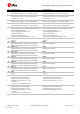
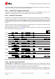
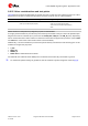
Table Of Contents
- Document information
- Contents
- 1 LARA-R2 / LARA-R6 modules description
- 2 Migration between LARA modules
- 2.1 Overview
- 2.2 Pin-out comparison between LARA modules
- 2.3 Interfaces comparison between LARA modules
- 2.3.1 VCC module supply input
- 2.3.2 V_INT 1.8 V supply output
- 2.3.3 V_BCKP RTC supply input/output
- 2.3.4 Cellular RF interfaces
- 2.3.5 System control interfaces
- 2.3.6 SIM interface
- 2.3.7 UART interfaces
- 2.3.8 USB interface
- 2.3.9 I2C interface
- 2.3.10 Digital audio interface
- 2.3.11 Clock output
- 2.3.12 GPIOs
- 2.3.13 Antenna dynamic tuning
- 2.3.14 Reserved pins
- 2.3.15 Other considerations and test points
- 2.4 Schematic for LARA modules integration
- Appendix
- A Glossary
- Related documents
- Revision history
- Contact

LARA-R2/R6 migration guide - Application note
UBX-21010015 - R02 Migration between LARA modules Page 15 of 25
C1-Public
2.3 Interfaces comparison between LARA modules
2.3.1 VCC module supply input
As the LARA-R2 and LARA-R6 series modules have compatible power requirements, there are only
minor differences in their VCC input voltage ranges and current consumption figures. The same
compatible external VCC supply circuit can be implemented for all the LARA modules, as for example
the one described in
Figure 4.
The nominal voltage provided at the VCC input pins must be within the related normal operating range
limits, and the actual voltage during module operations has to be held above the minimum limit of the
extended operating range to avoid the undervoltage switch-off of the module. For the detailed values
of VCC input voltage ranges, see
Table 5, or the related module’s data sheet [1] and [4].
The time-division RF transmission of 2G radio access technology can be up to ~2 W, whereas in 3G or
LTE radio access technology it is only up to ~0.25 W. Therefore, the pulse current profile in radio
connected mode when a data/voice call is enabled may be significantly higher for cellular modules
supporting the 2G radio access technology than for modules that do not have 2G fallback.
While selecting and designing the supply source for LARA cellular modules, consider with adequate
safe margin the maximum current consumption of the LARA cellular module specifically selected,
considering the radio access technologies supported by the module.
For the detailed module’s current consumption figures, see the related module’s data sheet [1] [4].
For additional specific design guidelines, see the related system integration manual [2] [5].
12V
10µF 10nF
22k
22pF
15k
VIN
RUN
VC
RT
PG
SYNC
BD
BOOST
SW
FB
GND
470nF
100nF330µF
390k
100k
10µH
680pF
LT3972
LARA-R2 / LARA-R6
VCC
VCC
VCC
GND
10nF 82pF 15pF 8.2pF
C ≥ 100 µF
for modules with
2G and/or LTE TDD
(C ~10 µF otherwise)
Ferrite Bead
BLM18EG221SN1
C = 8.2 pF 0402
for modules with
~2.6 GHz bands, as B7
(not needed otherwise)
For possible
VCC noise
suppression
(0R otherwise)
10µF
Close to
the regulator
Close to
the module
OFF ON
Figure 4: Example of compatible VCC supply application circuit using a high reliability step-down regulator
The VCC supply circuit illustrated in
Figure 4 includes capacitors with Self-Resonant Frequency in the
supported RF cellular bands, intended to be placed close to the VCC pins of the module, narrowing the
VCC line down to the pad of the capacitors, to adequately filter EMI in the supported RF cellular bands.
Additionally, a ferrite bead specifically designed to suppress EMI in the GHz band is placed very close
to the VCC pins of the module to suppress possible noise from the VCC line.
Note that the switch-on sequence of LARA-R2 series can be triggered by applying a valid VCC supply,
starting a voltage value of less than 2.1 V, and with a fast-rising slope (from 2.3 V to 2.8 V in less than
4 ms) up to the nominal VCC voltage within the normal operating range.
Instead, LARA-R6 series modules continue to be switched off even after a valid VCC supply has been
applied: the PWR_ON input line must be properly toggled low, with valid VCC supply present, to trigger
the switch-on sequence of these modules.
2.3.2 V_INT 1.8 V supply output
LARA-R2 and LARA-R6 series modules provide a 1.8 V supply output at the V_INT pin, which is
internally generated when the module is switched on.
The same voltage domain is used internally to supply the generic digital interfaces of the modules (as
the UARTs, I2C, I2S, GPIOs), and therefore it is recommended to use the V_INT supply output to
supply the module side of external voltage translators connected to these interfaces of the modules.