Revision 1.
Table Of Contents 1. Introduction....................................................................... 3 1.1 Overview................................................................3 1.2 Hardware Specifications..........................................4 1.3 Software Specifications.......................................... 5 1.4 Environment........................................................... 5 2. Board Installation.............................................................. 6 2.1 Unpacking........
1. Introduction 1.1 Overview The S1471 is a quality, high performance mainboard designed forl Intel Pentium microprocessors. This mainboard utilizes the Intel 430VX chipset and can support CPU speeds of 75MHz through 200MHz. S1470 will also support the CyrixM1/6x86 CPU's and the Intel multimedia Pentium P55C which utilizes MMX commands.
1.2 Hardware Specifications/Features wCPU Intel Pentium 75 MHz thru 200 MHz (Socket 7) Intel Pentium P55C Cyrix/IBM/SGS M1/6x86 P120, P150 & P166 wSpeed 50/60/66 MHz system bus 25/30/33 MHz PCI bus 7.5/8.33 MHz ISA bus speed wDRAM 2 banks of 72 pin SIMM and 2 DIMM Banks Supports 5V or 3.
wMouse On-board PS/2 mouse connector. 1.3 Software Specifications wBIOS Award or AMI BIOS AT CMOS setup, BIOS/CHIPSET setup, and hard disk utility included. Support for easy BIOS upgrades with flash EPROM chip. Operates with MS-DOS, Windows 3.x, Windows for Work Group 3.x, Windows 95, Windows NT OS/2, Novell Netware, and SCO Unix. wO.S. 1.
2. Board Installation 2.1 Unpacking The mainboard package should contain the following: wS1471 Mainboard wOne IDE 40 pin cables wTwo serial cables w One parallel cable wOne 34 pin floppy cable wUser's Manual The mainboard contains sensitive electric components which can be easily damaged by static electricity, so the mainboard should be left in its original packaging until it is ready to be installed.
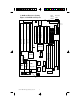
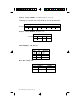
3. On Board Resource Setting Figure 3.1 S1471 Board Layout PS/2 Keyboard Mouse CON Header J13 J14 Super I/O PWR CON. 5V J 4 3 J41 J35 7 Secondary IDE Floppy Con. Parallel Port PCI Slot 1 Com1 Bank 1 SDRAM Bank 0 SDRAM Bank 1 DRAM 82438VX J 4 0J 3 9 S1471-001-01 http://www.tyan.com J8 JP1 JP2 J6 J3 Tag RAM J24 J23 J22 J21 J20 J42 pin 1 82438VX Regulator SRAM CPU SRAM Socket 7 JP5 Bank 0 DRAM Bank 1 DRAM pin 1 J15 Bank 0 DRAM JP4 Clock Gen.
3.
Memory Voltage SIMMs: Some EDO memory uses 3.3V. Damage to system can result if these are set incorrectly! Volts J5 Default 5V On 3.3V Off J7 On Off J9 On Off J11 On Off J3 Off On J6 Off On Memory Voltage DIMMs: Default is 5V. Volts Default 5V 3.3V JP1 1-2 2-3 JP2 1-2 2-3 JP3 1-2 2-3 J39 off off on on Multiplier x1.5 x2 x2.5 x3 CPU Multiplier: J40 and J39 J40 off on on off Host Bus Setting: J15 J15 1-2,3-4 1-2 3-4 S1471-001-01 http://www.tyan.com Host Speed 50MHz 66.
Reset Connector: J41 Pinout Assignment 1 Power Good 2 Ground Turbo LED Connector: J48 Pinout Assignment 1 Cathode 2 Anode Flash EPROM: J50 This jumper should be left at the factory default. J50 1-2 Keylock Connector: J47 Pinout Assignments 1 Led Output 2 No Connect 3 Ground 4 Keylock 5 Ground CMOS Resest/Password Reset: J45(Default off) If you at anytime need to reset the CMOS because you have forgotten your password do the following.
I/O Port Setting: J13 and J14 J13 Default For Serial Port 1-2 For IR Port 2-3 Speaker Connector: J42 Pinout Assignments 1 Speaker out 2 NC 3 Ground 4 + 5V Turbo Switch: J49 Non-Turbo mode not supported by chipset. Open for Turbo Close for Non-Turbo HDD LED: J43 Pinout Assignments 1 Cathode 2 Anode 3 Anode 4 Cathode Infra Red Interface: Con9 and Con10 Pinout 1 2 3 4 S1471-001-01 http://www.tyan.
3.3 CMOS RTC CMOS RTC includes an internal battery and Real Time Clock circuit. It provides the date and the time for the system. Normally the life span of a RTC internal battery is 10 years. When replacing, you should use the same model. 3.4 Speaker Connector Installation S1471 provides a 4-Pin header (J42) to connect the speaker. The polarity can go either way. 3.
3.7 Hardware Reset Switch Connector Installation The RESET switch on your cases' display panel provides users with the HARDWARE RESET functinon which is the same as power on/off. The system will do a cold start after the RESET switch is pushed by the user. The RESET switch is a 2 pin connector and should be installed on jumper J41. 3.8 Flash EPROM-Jumper J50 The S1471 uses flash memory to store BIOS programs. It can be updated as new versions of the BIOS becomes available.
3.9DRAM Installation The S1471 uses a 64-bit data path from memory to CPU and can accommodate up to 128 MB of RAM. The mainboard supports Fast Page Mode, and EDO (Extended Data Out) 72 pin SIMMs. SDRAM(Synchronous) are also supported in the DIMM slots. DIMM's must be of the unbuffered variety. All installed memory will be automatically detected so there is no need to set jumpers. wSIMM modules must be installed in pairs. wEach pair of SIMMs must be of the same size and type.
3.10 CPU Installation Several types of CPUs (75 thru 200MHz) can be used on S1471. Please refer to section 3.2 for the correct CPU jumper settings for your board. w The CPU is a sensitive electronic component and it can be easily damaged by static electricity. Do not touch the CPU pins with your fingers. w When installing the CPU into the socket, match the CPU pins to the socket pins. w Before the CPU is installed, the mainboard must be placed on a flat plane.
3.11 Upgrading Cache Memory The S1471 has either 256Kb or 512kb of on-board pipelined burst SRAM. Since the SRAM is surfaced mounted onto the board, the L2 Cache cannot be field upgraded. 3.12 Peripheral Device Installation After all the jumpers on the mainboard have been set, then it can be mounted into the case. Then proceed to install the display card and any other peripheral devices.
3.13 Connecting the Power Supply The system power supply connectors on the mainboard is for a 5 volt power supply. Incorrect installation of the power supply could result in serious damage to the system board and connected peripherals. Pin 1 Good Power Signal VCC 5 volt +12V power -12V GND connector pinout GND GND GND -5V VCC VCC VCC To connect the leads from either voltage power supply, you should first make sure the power supply is unplugged. Most power supplies have two leads.
Align the plastic guide pins on the lead cables to their receptacles on the mainboard. You may need to hold the lead at an angle to line it up.Once you have the guide pins aligned, press the lead connector so that the plastic clips on the lead snap into place and secure the lead to the connector. Connecting 5V power supply S1471-001-01 http://www.tyan.
4. BIOS Configuration Award's BIOS has a built in setup program that allows the user to modify the basic system configuration. This type of information is stored in the battery-backed CMOS SRAM. Entering incorrect information or forgetting your password can lock you out of your system.(refer to 3.9 for resetting of CMOS) 4.1. Entering Setup Power ON the computer and press immediately and you will enter Setup.
4.2.
4.3. Getting Help 4.3.1. Main Menu The on-line description of the highlighted setup function is displayed at the bottom of the screen. 4.3.2. Setup Page menu/Option Page Setup Menu Press F1 to pop up a small help window that describes the appropriate keys to use and the possible selections for the highlighted items. To exit the Help Window, press . 4.4. The Main Menu Once you enter the Award BIOS CMOS Setup Utility, the Main Menu (Figure 4.1) will appear on the screen.
w Standard CMOS setup This setup page includes all the items in a standard compatible BIOS. w BIOS features setup This setup page includes all of the enhanced features of Award's BIOS. w Chipset features setup This setup page includes all the items of the 430HX chipset features. w Power Management setup Change, set, or disable system power management options w PNP/PCI Configuration This setup page allows you to modify the configuration of PCI slot parameters.
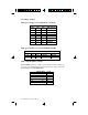
4.5. Standard CMOS Setup Menu The items in Standard CMOS Setup Menu (Figure 4.2) are divided into 9 categories. Each category includes one or more setup items. Use the arrows to highlight the item and use the or keys to select the value you want for each item. Figure 4.2: Standard CMOS Setup Menu ROM ISA BIOS (2A59CT51) STANDARD CMOS SETUP AWARD SOFTWARE, INC. Date (mm:dd:yy) : Tue, Dec 7 1995 Time (hh:mm:ss) : 18 : 01 : 38 Type Size CYLS. HEADS. PRECOMP.
w Primary/Secondary Drive type This category identifies the types of hard disk drives that have been installed in the computer. There are 46 predefined types and a user definable type. Press PgUp or PgDn to select a numbered hard disk type or type a number and press . Note that the specifications of your drive must match with the drive table. The hard disk will not work properly if you enter improper information for this category.
w Video This category detects the type of graphics adapter used for the primary display system. It must match your video display card and monitor. Although secondary monitors are supported, you do not have to select that type in setup. EGA/VGA CGA 40 CGA 80 Mono Enhanced Graphics Adapter/Video Graphics Array. For VGA,SVGA, or PGA monitor adapters. Color Graphics Adapter, power up in 40 column mode. Color Graphics Adapter, power up in 80 column mode. Monochrome adapter, includes hi-res monochrome.
Expanded Memory Expanded Memory (EMS) defines a 64Kb page frame in the area between 640K and 1Mb containing four 16K pages that are windows into the EMS memory. Programs issue requests to the EMS manager to switch the page to any part of EMS memory. Extended memory can be converted to emulate EMS by using a memory manager such as EMM386 that ships with Windows and DOS. Other Memory This refers to memory located in the 640K to 1024K ad dress space. This memory can be used for different applications.
w Virus warning This category flashes on screen. During and after the system boot up, any attempt to write to the boot sector or the partition table of the hard disk drive will halt the system and the following error message will appear. In the meantime, you can run an anti-virus program to locate the problem. Default value is Enabled. Enabled Activate automatically when the system boots up causing a warning message to appear when anything attemps to access the boot sector or hard disk partition table.
w Boot Up Floppy Seek During POST, the BIOS will determine if the floppy disk drive installed is 40 or 80 tracks. 360K type is 40 tracks while 720K, 1.2M and 1.44M are all 80 tracks. Default value is Enabled Enabled BIOS searches for floppy disk drive to determind if it is 40 or 80 tracks. Note that the BIOS cannot tell from 720k, 1.2M or 1.44M drive type as they are all 80 tracks Disabled BIOS will not search for the type of floppy disk drive by track number.
w Security Option This category allows you to limit access to the system setup, or just setup. Default value is Setup System The system will not boot and access to Setup will be denied if the correct password is not entered at the prompt Setup The system will boot, but access to setup will be denied if the password is not entered at the prompt w Video BIOS Shadow It determines whether Video BIOS will be copied to RAM, however, it is an optional chipset design. Default is Enabled. 4.
4.7.
w Doze Mode Defines the continous idle time before the system enters Doze mode. w Standby Mode Defines the continous idle time before the system enters Standby mode. w Power Down Activities Defines the the activities that can cause the PM timers to reload. (Breaking out of PM Mode) S1471-001-01 http://www.tyan.
4.8 PCI Slot Configuration ROM ISA BIOS PCI SLOT CONFIGURATION AWARD SOFTWARE, INC.
w Resources Controlled By The Award Plug and Play BIOS can automatically configure all the boot and Plug and Play compatible devices. If you seelect Auto, all the interrupt request and DMA assignment fields disappear, as the BIOS automatically assigns them. w IRQ n assigned to When resources are controlled manually, assign each system interrupt as one of the following types, depending on the type of device using the interrupt. Legacy ISA Devices compliant with the original PC AT bus specification.
4.9 Integrated Peripherals Integrated Peripherals Award Software, Inc.
4.9. LOAD SETUP DEFAULTS ROM ISA BIOS CMOS SETUP UTILITY AWARD SOFTWARE INC. STANDARD CMOS SETUP PASSWORD SETTING BIOS FEATURES SETUP IDE HDD AUTO DETECTION CHIPSET FEATURES SETUP DAVE & EXIT SETUP Load Setup Defaults (Y/N)? N PCI SLOT configuration EXIT WITH OUT SAVING LOAD SETUP DEFAULTS ESC : Save & Exit Setup F10 : Quit (Shift)F2 :Select Item :Change Color Load SETUP Defaults except standard CMOS SETUP w Load SETUP defaults To load SETUP default values to CMOS SRAM, enter "Y".
ROM ISA BIOS CMOS SETUP UTILITY AWARD SOFTWARE, INC. STANDARD CMOS SETUP PASSWORD SETTING BIOS FEATURES SETUP IDE HDD AUTO DETECTION CHIPSET FEATURES SETUP DAVE & EXIT SETUP Enter Password PCI SLOT CONFIGURATION EXIT WITH OUT SAVING LOAD SETUP DEFAULTS ESC : Save & Exit Setup F10 : Quit (Shift)F2 :Select Item :Change Color Change/Set/Disable Password Type the password, up to eight characters, and press . The password typed now will clear the previously entered password from CMOS memory.
4.11. IDE HDD AUTO DETECTION ROM ISA BIOS CMOS SETUP UTILITY AWARD SOFTWARE, INC. CYLS. Drive C: (202 Mb) HEAD 989 12 PRECOMP LANZONE 65535 989 SECTORS 35 Do you want to accept this as drive C (Y/N)? Esc:Skip Type "Y" to accept the H.D.D parameter reported by BIOS. Type "N" to keep the old H.D.D parameter info. 4.12. SAVE & EXIT SETUP ROM ISA BIOS CMOS SETUP UTILITY AWARD SOFTWARE, INC.
5.0 Flash Writer Utility Warning: Do not flash the BIOS unless instructed by your dealer. You can upgrade the BIOS of your mainboard by using a "Flash Memory Writer"(FMW) utility. This utility can be downloaded from Tyan's BBS(Consult your system vendor for the phone #) or web site. The system BIOS is stored on a 'flash' EPROM ROM chip on the mainboard which can be erased and reprogrammed by the FMW. The following three files make up the FMW. AWDFLASH.EXE AMIFLASH.COM README *S71AWXX.
To reprogram the System BIOS, you must first do the following: 1. Check jumper J50.(Default pins 1-2) The S1471 uses a 5V Flash EPROM so jumper J50 should be left in the default postion on pins 1 and 2. This jumper should never be moved. 2. Make sure the CPU is running in ‘real mode’. FMW will not run if the CPU is operating in a protected or virtual mode. This means that you can not run it with Windows running or with any memory manager software. You must disable any memory manager first.
Once you have satisfied the two requirements mentioned above, you can run FMW. You can copy the contents of the “Flash” directory to your hard drive, or you can run the utility from a backup of the support floppy disk. Make sure the new BIOS file is in the same directory as the FMW utility. To run FMW, change to the “Flash” directory if you are not already in it. Type “Awdflash” at the DOS command line and press the key. The following screen will appear. 5.
6.0 System Resource 6.1. TIMER & DMA CHANNEL MAP TIMER MAP: TIMER Channel-0 system timer interrupt TIMER Channel-1 DRAM REFRESH request TIMER Channel-2 SPEAKER tone generator DMA CHANNELS: DMA Channel-0 Available DMA Channel-1 Available DMA Channel-2 FLOPPY DISK adapter DMA Channel-3 Available DMA Channel-4 Cascade for DMA controller 1 DMA Channel-5 Available DMA Channel-6 Available DMA Channel-7 Available 6.