
User's Manual
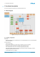
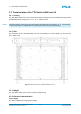

Table Of Contents
- Front Cover
- Table of Contents
- List of Tables
- List of Figures
- Disclaimer
- Limited Rights Notice
- 1 Introduction
- 2 Overview
- 3 Functional description
- 4 Getting started
- 5 State machine
- 6 Creating a switch configuration
- 7 Diagnosis
- 8 Troubleshooting
- Appendix A List of Built-In Self-Tests
- Appendix B Serial terminal output at start-up
- Glossary
- References
- Index

3. FUNCTIONAL DESCRIPTION
≡
3 Functional description
This section describes the functionality of the TTE-Switch A664 Lab v2.0.
3.1 Block diagram
Figure 5: Block diagram of the TTE-Switch A664 Lab v2.0
3.1.1 Primary components
Base Board:
• 25 Ethernet transceivers (18 x 10/100 Mbit/s ports, 6 x 10/100/1000 Mbit/s ports, and 1 x 10/100/1000 Mbit/s
port for mirroring only).
TTE Switch Module 2:
• ASIC as switch engine.
• Reduced-latency DRAM with a storage capacity of 288 Mbit and running at 320 MHz.
• Application CPU that controls BISTs, error logging and management functions.
• Three 256 Mbit Flash memory ICs for storing the configuration(s) (CPU Flash).
• JTAG chain that offers access to the CPU and reduced-latency DRAM for debugging, production
testing and programming the flash memories.
• A 64 kbit FRAM used for error logging.
© TTTech Computertechnik AG 2020. All rights reserved.
Confidential and Proprietary Information
10
Document Number:
D-A664Lab-G-05-001