
Datasheet


TMC2660 DATASHEET (Rev. 1.01 / 2013-AUG-01) 53
www.trinamic.com
21 Table of Figures
Figure 1.1 Block diagram: applications........................................................................................................................... 4
Figure 2.1 TMC2660 pin assignment................................................................................................................................ 6
Figure 3.1 TMC2660 block diagram .................................................................................................................................. 8
Figure 4.1 stallGuard2 load measurement SG as a function of load .................................................................... 9
Figure 4.2 Linear interpolation for optimizing SGT with changes in velocity. ................................................. 10
Figure 5.1 Energy efficiency example with coolStep ................................................................................................ 12
Figure 5.2 coolStep adapts motor current to the load. ........................................................................................... 13
Figure 6.1 SPI Timing ........................................................................................................................................................ 15
Figure 6.2 Interfaces to a TMC429 motion controller chip and a TMC2660 motor driver ............................. 16
Figure 7.1 STEP and DIR timing. .................................................................................................................................... 26
Figure 7.2 Internal microstep table showing the first quarter of the sine wave. .......................................... 27
Figure 7.3 microPlyer microstep interpolation with rising STEP frequency. ..................................................... 28
Figure 8.1 Sense resistor grounding and protection components ...................................................................... 31
Figure 9.1 Chopper phases. ............................................................................................................................................. 32
Figure 9.2 spreadCycle chopper mode showing the coil current during a chopper cycle ........................... 34
Figure 9.3 Constant off-time chopper with offset showing the coil current during two cycles, ............... 35
Figure 9.4 Zero crossing with correction using sine wave offset. ....................................................................... 35
Figure 11.1 Short to GND detection timing. ............................................................................................................... 38
Figure 11.2 Undervoltage reset timing ......................................................................................................................... 40
Figure 15.1 Layout example 1 for TMC2660 ................................................................................................................ 44
Figure 15.2 Layout example 2 for TMC2660 ................................................................................................................ 45
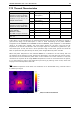
Figure 17.1 TMC2660 operating at 2.3A RMS (3.2A peak) on a 50cm² sized board ......................................... 50
Figure 18.1 Dimensional drawings (PQFP44) .............................................................................................................. 51