
Datasheet


TMC260/A and TMC261 DATASHEET (Rev. 2.10 / 2016-JUL-14) 45
www.trinamic.com
16 Absolute Maximum Ratings
The maximum ratings may not be exceeded under any circumstances. Operating the circuit at or near
more than one maximum rating at a time for extended periods shall be avoided by application
design.
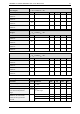
Parameter
Symbol
Min
Max
Unit
Supply voltage (TMC261)
V
VS
-0.5
60
V
Supply voltage (TMC260)
-0.5
40
V
Logic supply voltage
V
VCC
-0.5
6.0
V
I/O supply voltage
V
VIO
-0.5
6.0
V
Logic input voltage
V
I
-0.5
V
VIO
+0.5
V
Analog input voltage
V
IA
-0.5
V
CC
+0.5
V
Relative high-side gate driver voltage (V
VM
– V
HS
)
V
HSVM
-0.5
15
V
Maximum current to/from digital pins
and analog low voltage I/Os
I
IO
+/-10
mA
Non-destructive short time peak current into input/output pins
I
IO
500
mA
Bridge output peak current (10µs pulse)
I
OP
+/-7
A
Output current, continuous
(one bridge active, or 0.71 x current with
both bridges active)
T
A
≤ 50°C
I
OC
2000
mA
T
A
≤ 85°C
1500
T
A
≤ 105°C
1100
T
A
≤ 125°C
800
5V regulator output current
I
5VOUT
50
mA
5V regulator peak power dissipation (V
VM
-5V) * I
5VOUT
P
5VOUT
1
W
Junction temperature
T
J
-50
150
°C
Storage temperature
T
STG
-55
150
°C
ESD-Protection (Human body model, HBM), in application
V
ESDAP
1
kV
ESD-Protection (Human body model, HBM), device handling
V
ESDDH
300
V