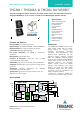
POWER DRIVER FOR STEPPER MOTORS INTEGRATED CIRCUITS TMC260 / TMC260A & TMC261 DATASHEET Universal, cost-effective stepper drivers for two-phase bipolar motors with state-of-the-art features. Integrated MOSFETs for up to 2 A motor currents per coil. With Step/Dir Interface and SPI.
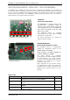
TMC260/A and TMC261 DATASHEET (Rev. 2.10 / 2016-JUL-14) 2 APPLICATION EXAMPLES: SMALL SIZE – BEST PERFORMANCE The TMC260 and the TMC261 score with power density, integrated power MOSFETs, and a versatility that covers a wide spectrum of applications and motor sizes, all while keeping costs down. Extensive support at the chips, board, and software levels enables rapid design cycles and fast time-to-market with competitive products.
TMC260/A and TMC261 DATASHEET (Rev. 2.10 / 2016-JUL-14) 3 TABLE OF CONTENTS 1 PRINCIPLES OF OPERATION ............... 4 1.1 1.2 1.3 1.4 2 2.1 2.2 12 POWER SUPPLY SEQUENCING .......... 41 PIN ASSIGNMENTS ................................. 6 13 SYSTEM CLOCK ...................................... 41 PACKAGE OUTLINE ......................................... 6 SIGNAL DESCRIPTIONS .................................. 6 INTERNAL ARCHITECTURE.................... 8 4 STALLGUARD2 LOAD MEASUREMENT 9 4.3 4.
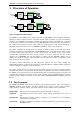
TMC260/A and TMC261 DATASHEET (Rev. 2.10 / 2016-JUL-14) 1 4 Principles of Operation 0A+ High-Level Interface µC S/D TMC260 TMC261 0A- S N 0B+ 0B- SPI 0A+ TMC429 µC High-Level Interface SPI Motion Controller for up to 3 Motors S/D TMC260 TMC261 0A- S N 0B+ 0B- SPI Figure 1.1 applications block diagram The TMC260 and the TMC261 motor driver chips with included MOSFETs are intelligence and power between a motion controller and the two phase stepper motor as shown in Figure 1.1.
TMC260/A and TMC261 DATASHEET (Rev. 2.10 / 2016-JUL-14) 5 In addition to these performance enhancements, TRINAMIC motor drivers also offer safeguards to detect and protect against shorted outputs, open-circuit output, overtemperature, and undervoltage conditions for enhancing safety and recovery from equipment malfunctions. 1.2 Control Interfaces There are two control interfaces from the motion controller to the motor driver: the SPI serial interface and the STEP/DIR interface.
TMC260/A and TMC261 DATASHEET (Rev. 2.10 / 2016-JUL-14) Pin Assignments GND TST_MODE STEP DIR VCC_IO GND SG_TST TST_ANA VS VHS - 43 42 41 40 39 38 37 36 35 34 4 30 5 29 TMC260-PA / TMC261-PA QFP44 6 7 28 27 19 20 21 22 - CLK SRB 23 18 24 11 CSN 10 ENN 25 17 9 SCK 26 GND 8 16 OA2 31 15 BRA 3 SDI OA1 32 14 OA2 2 13 VSA 33 SDO OA1 1 5VOUT - 44 Package Outline 12 2.1 SRA 2 6 OB1 VSB OB2 OB1 BRB OB2 Figure 2.
TMC260/A and TMC261 DATASHEET (Rev. 2.10 / 2016-JUL-14) Pin SDI Number 15 Type DI VIO SCK 16 DI VIO GND CSN ENN 17, 39, 44 18 19 DI VIO DI VIO CLK 21 DI VIO VHS VS TST_ANA SG_TST VCC_IO 35 36 37 38 40 DIR 41 DI VIO STEP 42 DI VIO TST_MODE 43 DI VIO n.c. 1, 33 www.trinamic.com AO VIO DO VIO 7 Function SPI serial data input. (Scan test input in test mode.) Serial clock input of SPI interface. (Scan test shift enable input in test mode.) Digital and analog low power GND.
TMC260/A and TMC261 DATASHEET (Rev. 2.10 / 2016-JUL-14) 3 8 Internal Architecture Figure 3.1 shows the internal architecture of TMC26O and TMC261. +VM 9-39V / 9-59V VHS 100n 16V 100n VS TMC260 / TMC261 +VCC VCC_IO 3.
TMC260/A and TMC261 DATASHEET (Rev. 2.10 / 2016-JUL-14) 4 9 stallGuard2 Load Measurement stallGuard2 provides an accurate measurement of the load on the motor. It can be used for stall detection as well as other uses at loads below those which stall the motor, such as coolStep loadadaptive current reduction. (stallGuard2 is a more precise evolution of the earlier stallGuard technology.
TMC260/A and TMC261 DATASHEET (Rev. 2.10 / 2016-JUL-14) Status word SG 4.1 10 Description 10-bit unsigned integer stallGuard2 measurement value. A higher value indicates lower mechanical load. A lower value indicates a higher load and therefore a higher load angle. For stall detection, adjust SGT to return an SG value of 0 or slightly higher upon maximum motor load before stall.
TMC260/A and TMC261 DATASHEET (Rev. 2.10 / 2016-JUL-14) 11 4.1.2 Small Motors with High Torque Ripple and Resonance Motors with a high detent torque show an increased variation of the stallGuard2 measurement value SG with varying motor currents, especially at low currents. For these motors, the current dependency might need correction in a similar manner to velocity correction for obtaining the highest accuracy. 4.1.
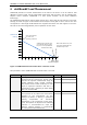
TMC260/A and TMC261 DATASHEET (Rev. 2.10 / 2016-JUL-14) 5 12 coolStep Load-Adaptive Current Control coolStep allows substantial energy savings, especially for motors which see varying loads or operate at a high duty cycle. Because a stepper motor application needs to work with a torque reserve of 30% to 50%, even a constant-load application allows significant energy savings because coolStep automatically enables torque reserve when required.
TMC260/A and TMC261 DATASHEET (Rev. 2.10 / 2016-JUL-14) 13 mechanical load stallGuard2 reading motor current increases the current. When the load decreases and SG rises above (SEMIN + SEMAX + 1) x 32 the current becomes reduced.
TMC260/A and TMC261 DATASHEET (Rev. 2.10 / 2016-JUL-14) 5.1 14 Tuning coolStep Before tuning coolStep, first tune the stallGuard2 threshold level SGT, which affects the range of the load measurement value SG. coolStep uses SG to operate the motor near the optimum load angle of +90°. The current increment speed is specified in SEUP, and the current decrement speed is specified in SEDN. They can be tuned separately because they are triggered by different events that may need different responses.
TMC260/A and TMC261 DATASHEET (Rev. 2.10 / 2016-JUL-14) 6 15 SPI Interface TMC260 and TMC261 require setting configuration parameters and mode bits through the SPI interface before the motor can be driven. The SPI interface also allows reading back status values and bits. 6.
TMC260/A and TMC261 DATASHEET (Rev. 2.
TMC260/A and TMC261 DATASHEET (Rev. 2.10 / 2016-JUL-14) 6.
TMC260/A and TMC261 DATASHEET (Rev. 2.10 / 2016-JUL-14) 18 6.4.2 Read Response Overview The table below shows the formats for the read response. The RDSEL parameter in the DRVCONF register selects the format of the read response. 6.
TMC260/A and TMC261 DATASHEET (Rev. 2.10 / 2016-JUL-14) DRVCTRL Driver Control in SPI Mode (SDOFF=1) Bit 8 Name PHB Function Polarity B CB7 CB6 CB5 CB4 CB3 CB2 CB1 CB0 Current B MSB 7 6 5 4 3 2 1 0 19 Comment Sign of current flow through coil B: 0: Current flows from OB1 pins to OB2 pins. 1: Current flows from OB2 pins to OB1 pins. Magnitude of current flow through coil B. The range is 0 to 248, if hysteresis or offset are used up to their full extent.
TMC260/A and TMC261 DATASHEET (Rev. 2.10 / 2016-JUL-14) 6.6 Chopper Control Register (CHOPCONF) CHOPCONF Chopper Configuration Bit 19 18 17 16 15 Name 1 0 0 TBL1 TBL0 Function Register address bit Register address bit Register address bit Blanking time CHM Chopper mode 14 20 Comment Blanking time interval, in system clock periods: %00: 16 %01: 24 %10: 36 %11: 54 This mode bit affects the interpretation of the HDEC, HEND, and HSTRT parameters shown below.
TMC260/A and TMC261 DATASHEET (Rev. 2.10 / 2016-JUL-14) CHOPCONF Chopper Configuration Bit 3 2 1 0 Function Off time/MOSFET disable 6.7 Name TOFF3 TOFF2 TOFF1 TOFF0 21 Comment Duration of slow decay phase. If TOFF is 0, the MOSFETs are shut off. If TOFF is nonzero, slow decay time is a multiple of system clock periods: NCLK= 12 + (32 x TOFF) (Minimum time is 64clocks.
TMC260/A and TMC261 DATASHEET (Rev. 2.10 / 2016-JUL-14) 6.8 22 stallGuard2 Control Register (SGCSCONF) SGCSCONF stallGuard2™ and Current Setting Bit 19 18 17 16 Name 1 1 0 SFILT Function Register address bit Register address bit Register address bit stallGuard2 filter enable 15 14 13 12 11 10 9 8 7 6 5 4 3 2 1 0 0 SGT6 SGT5 SGT4 SGT3 SGT2 SGT1 SGT0 0 0 0 CS4 CS3 CS2 CS1 CS0 Reserved stallGuard2 threshold value www.trinamic.
TMC260/A and TMC261 DATASHEET (Rev. 2.10 / 2016-JUL-14) 6.
TMC260/A and TMC261 DATASHEET (Rev. 2.10 / 2016-JUL-14) 24 6.10 Read Response For every write command sent to the motor driver, a 20-bit response is returned to the motion controller. The response has one of three formats, as selected by the RDSEL parameter in the DRVCONF register. The table below shows these formats. Software must not depend on the value of any bit shown as reserved.
TMC260/A and TMC261 DATASHEET (Rev. 2.10 / 2016-JUL-14) 25 6.11 Device Initialization The following sequence of SPI commands is an example of enabling the driver and initializing the chopper: SPI = $901B4; // Hysteresis mode SPI = $94557; // Constant toff mode SPI = $D001F; // Current setting: $d001F (max.
TMC260/A and TMC261 DATASHEET (Rev. 2.10 / 2016-JUL-14) 7 26 STEP/DIR Interface The STEP and DIR inputs provide a simple, standard interface compatible with many existing motion controllers. The microPlyer STEP pulse interpolator brings the smooth motor operation of highresolution microstepping to applications originally designed for coarser stepping and reduces pulse bandwidth. 7.1 Timing Figure 7.
TMC260/A and TMC261 DATASHEET (Rev. 2.10 / 2016-JUL-14) 7.2 27 Microstep Table The internal microstep table maps the sine function from 0° to 90°, and symmetries allow mapping the sine and cosine functions from 0° to 360° with this table. The angle is encoded as a 10-bit unsigned integer MSTEP provided by the microstep counter. The size of the increment applied to the counter while microstepping through this table is controlled by the microstep resolution setting MRES in the DRVCTRL register.
TMC260/A and TMC261 DATASHEET (Rev. 2.10 / 2016-JUL-14) 7.3 28 Changing Resolution The application may need to change the microstepping resolution to get the best performance from the motor. For example, high-resolution microstepping may be used for precision operations on a workpiece, and then fullstepping may be used for maximum torque at maximum velocity to advance to the next workpiece.
TMC260/A and TMC261 DATASHEET (Rev. 2.10 / 2016-JUL-14) 29 In Figure 7.3, the first STEP cycle is long enough to set the STST bit. This bit is cleared on the next STEP active edge. Then, the STEP frequency increases and after one cycle at the higher rate microPlyer increases the interpolated microstep rate. During the last cycle at the slower rate, microPlyer did not generate all 16 microsteps, so there is a small jump in motor angle between the first and second cycles at the higher rate. 7.
TMC260/A and TMC261 DATASHEET (Rev. 2.10 / 2016-JUL-14) 8 30 Current Setting The internal 5V supply voltage available at the pin 5VOUT is used as a reference for the coil current regulation based on the sense resistor voltage measurement. The desired maximum motor current is set by selecting an appropriate value for the sense resistor. The sense resistor voltage range can be selected by the VSENSE bit in the DRVCONF register.
TMC260/A and TMC261 DATASHEET (Rev. 2.10 / 2016-JUL-14) 8.1 31 Sense Resistors Sense resistors should be carefully selected. The full motor current flows through the sense resistors. They also see the switching spikes from the MOSFET bridges. A low-inductance type such as film or composition resistors is required to prevent spikes causing ringing on the sense voltage inputs leading to unstable measurement results. A low-inductance, low-resistance PCB layout is essential.
TMC260/A and TMC261 DATASHEET (Rev. 2.10 / 2016-JUL-14) 9 32 Chopper Operation The currents through both motor coils are controlled using choppers. The choppers work independently of each other. Figure 9.1 shows the three chopper phases: +VM +VM +VM ICOIL ICOIL ICOIL RSENSE RSENSE On Phase: current flows in direction of target current Fast Decay Phase: current flows in opposite direction of target current RSENSE Slow Decay Phase: current re-circulation Figure 9.1 Chopper phases.
TMC260/A and TMC261 DATASHEET (Rev. 2.10 / 2016-JUL-14) Parameter TBL CHM 9.1 33 Description Blanking time. This time needs to cover the switching event and the duration of the ringing on the sense resistor. For most low-current applications, a setting of 16 or 24 is good. For high-current applications, a setting of 36 or 54 may be required.
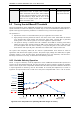
TMC260/A and TMC261 DATASHEET (Rev. 2.10 / 2016-JUL-14) 34 An Excel spreadsheet is provided for performing these calculations. As experiments show, the setting is quite independent of the motor, because higher current motors typically also have a lower coil resistance. Choosing a medium default value for the hysteresis (for example, effective HSTRT+HEND=10) normally fits most applications.
TMC260/A and TMC261 DATASHEET (Rev. 2.10 / 2016-JUL-14) Parameter HDEC 35 Description Setting Hysteresis decrement setting. This setting 0… 3 determines the slope of the hysteresis during on time and during fast decay time. It sets the number of system clocks for each decrement. Comment 0: fast decrement 3: very slow decrement %00: 16 %01: 32 %10: 48 %11: 64 Example: In the example above, a hysteresis start of 7 has been chosen. The hysteresis end is set to about half of this value, 3.
TMC260/A and TMC261 DATASHEET (Rev. 2.10 / 2016-JUL-14) 36 Three parameters control constant off-time mode: Parameter TFD (HSTART & HDEC0) OFFSET (HEND) NCCFD (HDEC1) Description Fast decay time setting. With CHM=1, these bits control the portion of fast decay for each chopper cycle. Sine wave offset. With CHM=1, these bits control the sine wave offset. A positive offset corrects for zero crossing error. Selects usage of the current comparator for termination of the fast decay cycle.
TMC260/A and TMC261 DATASHEET (Rev. 2.10 / 2016-JUL-14) 37 10 Power MOSFET Stage The gate current for the power MOSFETs can be adapted to influence the slew rate at the coil outputs. The main features of the stage are: - 5V gate drive voltage for low-side N-MOS transistors, 8V for high-side P-MOS transistors. - The gate drivers protect the bridges actively against cross-conduction using an internal QGD protection that holds the MOSFETs safely off.
TMC260/A and TMC261 DATASHEET (Rev. 2.10 / 2016-JUL-14) 38 11 Diagnostics and Protection 11.1 Short to GND Detection The short to ground detection prevents the high-side power MOSFETs from being damaged by accidentally shorting the motor outputs to ground. It disables the MOSFETs only if a short condition persists. A temporary event like an ESD event could look like a short, but these events are filtered out by requiring the event to persist.
TMC260/A and TMC261 DATASHEET (Rev. 2.10 / 2016-JUL-14) 39 The short to ground detector is controlled by a mode bit and a parameter: Mode bit / Parameter DISS2G Description Setting Comment Short to ground detection disable bit. 0/1 TS2G This setting controls the short to GND detection 0… 3 delay time. It needs to cover the switching slope time. A higher setting reduces sensitivity to capacitive loads. 0: Short to ground detection enabled. 1: Short to ground detection disabled. %00: 3.2µs. %01: 1.
TMC260/A and TMC261 DATASHEET (Rev. 2.10 / 2016-JUL-14) Status OTPW 40 Description Range Overtemperature warning. This bit indicates 0 / 1 whether the warning threshold is reached. Software can react to this setting by reducing current. Overtemperature shutdown. This bit indicates 0 / 1 whether the shutdown threshold has been reached and the driver has been disabled. OT Comment 1: temperature prewarning level reached 1: driver shut down due to overtemperature 11.
TMC260/A and TMC261 DATASHEET (Rev. 2.10 / 2016-JUL-14) 41 12 Power Supply Sequencing The TMC260 and TMC261 generate their own 5V supply for all internal operations. The internal reset of the chips is derived from the supply voltage regulators in order to ensure a clean start-up of the devices after power up. During start up, the SPI unit is in reset and cannot be addressed. All registers become cleared.
VVCC_IO VCLK 3.3V/5V VINHI CLK must be low, while VCC_IO is below VINHI TMC260/A and TMC261 DATASHEET (Rev. 2.10 / 2016-JUL-14) Defined clock, no intermediate levels allowed 42 max. VCC_IO VVS VUV Device in reset: all registers cleared to 0 Operation, CLK is not allowed to have undefined levels between VINLO and VINHI and timing must satisfy TCLK (min) Time Device in reset: all registers cleared to 0 Figure 13.1 Start-up requirements of CLK input 13.
TMC260/A and TMC261 DATASHEET (Rev. 2.10 / 2016-JUL-14) 43 15 Layout Considerations The PCB layout is critical to good performance, because the environment includes both highsensitivity analog signals and high-current motor drive signals. 15.1 Sense Resistors The sense resistors are susceptible to ground differences and ground ripple voltage, as the microstep current steps result in voltages down to 0.5mV. No current other than the sense resistor currents should flow through their connections to ground.
TMC260/A and TMC261 DATASHEET (Rev. 2.10 / 2016-JUL-14) 44 15.4 Layout Example EXAMPLE FOR UP TO 2.8A RMS Here, an example for a layout with small board size (≈20cm²) is shown. top layer (assembly side) inner layer inner layer bottom layer (solder side) Figure 15.1 Layout example for TMC260 and TMC261 www.trinamic.
TMC260/A and TMC261 DATASHEET (Rev. 2.10 / 2016-JUL-14) 45 16 Absolute Maximum Ratings The maximum ratings may not be exceeded under any circumstances. Operating the circuit at or near more than one maximum rating at a time for extended periods shall be avoided by application design.
TMC260/A and TMC261 DATASHEET (Rev. 2.10 / 2016-JUL-14) 46 17 Electrical Characteristics 17.1 Operational Range Parameter Junction temperature Supply voltage TMC261 Supply voltage TMC260 I/O supply voltage Symbol Min Max Unit TJ VVS VVS VVIO -40 9 9 3.00 125 59 39 5.25 °C V V V 17.2 DC and AC Specifications DC characteristics contain the spread of values guaranteed within the specified supply voltage range unless otherwise specified.
TMC260/A and TMC261 DATASHEET (Rev. 2.10 / 2016-JUL-14) Internal MOSFETs TMC260 (non-A-Type) DC Characteristics VVS = VVSX ≥ 12.0V, VBRX = 0V Parameter Symbol Conditions N-channel MOSFET on resistance P-channel MOSFET on resistance N-channel MOSFET on resistance P-channel MOSFET on resistance Typ Max Unit TJ = 25°C 125 190 mΩ RONP TJ = 25°C 190 240 mΩ RONN TJ = 150°C 205 mΩ RONP TJ = 150°C 312 mΩ DC Characteristics VVS = VVSX ≥ 12.
TMC260/A and TMC261 DATASHEET (Rev. 2.10 / 2016-JUL-14) Clock Oscillator and CLK Input Timing Characteristics Parameter Symbol Conditions Clock oscillator frequency Clock oscillator frequency Clock oscillator frequency External clock frequency (operating) External clock high / low level time fCLKOSC fCLKOSC fCLKOSC fCLK tJ=-50°C tJ=50°C tJ=150°C tCLK Parameter Symbol Conditions Overtemperature warning Overtemperature shutdown VUV VBMS2G tOTPW tOT Typ 10.0 10.8 14.3 15.2 15.4 Max 20.0 20.
TMC260/A and TMC261 DATASHEET (Rev. 2.10 / 2016-JUL-14) 49 17.
TMC260/A and TMC261 DATASHEET (Rev. 2.10 / 2016-JUL-14) 50 18 Package Mechanical Data 18.1 Dimensional Drawings Attention: Drawings not to scale. E F G D C A I H K Figure 18.1 Dimensional drawings (PQFP44) Parameter Ref Size over pins (X and Y) A Body size (X and Y) C Pin length D Total thickness E Lead frame thickness F Stand off G Pin width H Flat lead length I Pitch K Coplanarity ccc Min 0.09 0.05 0.30 0.45 Nom 12 10 1 0.10 Max 1.6 0.2 0.15 0.45 0.75 0.8 0.08 18.
TMC260/A and TMC261 DATASHEET (Rev. 2.10 / 2016-JUL-14) 51 19 Disclaimer TRINAMIC Motion Control GmbH & Co. KG does not authorize or warrant any of its products for use in life support systems, without the specific written consent of TRINAMIC Motion Control GmbH & Co. KG. Life support systems are equipment intended to support or sustain life, and whose failure to perform, when properly used in accordance with instructions provided, can be reasonably expected to result in personal injury or death.
TMC260/A and TMC261 DATASHEET (Rev. 2.10 / 2016-JUL-14) 52 21 Table of Figures Figure Figure Figure Figure Figure Figure Figure Figure Figure Figure Figure Figure Figure Figure Figure Figure Figure Figure Figure Figure Figure Figure Figure 1.1 applications block diagram ............................................................................................................................ 4 2.1 TMC260/261 pin assignments. ...............................................................................
TMC260/A and TMC261 DATASHEET (Rev. 2.10 / 2016-JUL-14) 53 22 Revision History Version Date Author Description BD = Bernhard Dwersteg SD – Sonja Dwersteg 0.94 1.00 2010-APR-22 2010-AUG-09 BD BD 1.07 2010-NOV-22 BD 1.08 1.10 1.11 1.12 1.13 1.15 1.17 2.00 2010-DEC-01 2011-MAR-09 2011-APR-12 2011-JUL-26 2011-OKT-05 2011-DEC-14 2012-JAN-18 2012-MAR-29 BD BD BD BD BD BD BD SD 2.01 2012-JUN-07 SD 2.02 2012-AUG-01 SD 2.03 2.04 2.05 2012-AUG-13 2012-AUG-30 2012-NOV-05 SD SD SD 2.