
User manual


TMCM-1110 stepRocker Hardware Manual (Ref. 1.08 / 2012-APR-04) 9
www.trinamic.com
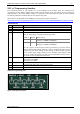
3.2.9 µC Programming Interface
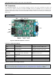
The programming pads of the interface are on the backside of the module. There are possibilities for
programming in two different modes: debug mode and serial writing mode. The selection of the programming
mode depends on the chosen adapter. Further, it is possible to use the programming pads of the µC interface
by soldering adequate contacts directly on the programming pads.
Please refer to the datasheet of the S3FN41F microcontroller for further information.
http://www.samsung.com/global/system/business/semiconductor/product/2011/6/21/024872um_s3fn41f_rev10.pdf
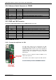
PROGRAMMING PADS
Pin
Label
Description
1
GND
Module and signal ground
2
+5V
+5V DC supply
3
nRST
Hardware reset input
4
VPP
Connected to pin 14 of the processor (MODE0). VPP is used for mode setting
ether to debug mode or to flash serial writing mode.
Mode 1
Mode 0
Mode setting
0
0
User normal/debug mode.
(Used pins: SWDIO and SWDCLK.)
0
1
User flash serial writing mode.
(Used pins: F_SDAT and PHASEA.)
The user program mode for flash memory programming and sector erasing
uses the internal high voltage generator, which is necessary for flash memory
programming and sector erasing. In other words, the flash memory controller
has an internal high voltage pumping circuit. Therefore, high voltage to VPP
pin is not needed. To program the data into the flash ROM or sector erase in
this mode, control registers should be used.
5
PHASEA
Function: F_CLK – serial clock.
Write speed: max 250kHz
Read speed: max 3MHz
6
F_SDAT
Serial Data pin (output for reading, input for writing)
Input and push-pull output port can be assigned.
7
SWDIO
Select/Serial Wire Data I/O. Internal pull-up
8
SWDCLK
Serial wire clock
Table 3.3: Programming pads
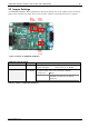
GND
+5V
nRST
VPP
PHASEA
F SDAT
SWDIO
SWDCLK
1
Figure 3.2: Programming pads