
User's Guide


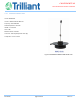


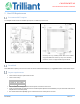
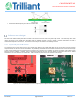
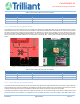

Table Of Contents
- 1 Overview
- 2 Features and Specifications
- 3 Functional Description
- 4 Antennas
- 5 Host PCB Requirements
- 6 SecureMesh Configuration
- 7 Regulatory Agency Approvals

DT-0237A page 17 of 34 Rev: 1.2
CONFIDENTIAL
DISTRIBUTED UNDER LICENSE
5 Host PCB Requirements
Recommended Footprint
The footprints shown below are available upon request as a PAD Layout source file.
OSDI-4000-1X
•
Overall (L x W x H), including shield: 29.8 x 35.3 x 4.0mm
•
Suggested Silkscreen Outline (L x W): 30.3 x 35.8mm
•
Avoid vias, traces or copper inside Keep-Out Areas
Figure 15 Footprint OSDI-4000-1X
PasteMask
Paste Mask Stencil openings can be of the same size as the recommended footprint (1:1); suggested thickness of stencil foil ≥ 120µm.
Layout requirements
• Traces routed to RF_EXT pad must be 50 ohm.
• Traces current rating:
+VCPU
≥ 90 mA
+3.3V
≥ 90 mA
+VLDO_IN
≥ 1.4 Amp
+V1.5F_SW
≥ 90mA
• Thermal reliefs are strongly recommended for all pads connected to Ground net.
• Finish recommendation for PCB pad surfaces: ROHS Compliant (EU Directive 2002/95/EC) 2-10 µIN Immersion Gold Over 50-
200µIN Electro less Nickel (ENIG)
• Non Solder Mask Defined (NSMD) type is recommended for the solder pads on the PCB.