
Datasheet


T
T
T
S
S
S
6
6
6
4
4
4
M
F
M
M
L
L
L
D
D
D
6
6
6
4
4
4
V
V
V
5
5
5
F
F
184PIN DDR500 Unbuffered DIMM
512MB With 32Mx8 CL3
Transcend Information Inc.
7
AC OPERATING CONDITIONS
Parameter
Input Levels (VIH/VIL) VREF+0.31/VREF-0.31
Symbol Min Max
Unit
V
Input timing measurement reference level
Note
Input High (Logic 1) Voltage, DQ, DQS and DM signals
VREF V
VIH(AC) VREF + 0.31
Output timing measurement reference level VTT
V
Input Low (Logic 0) Voltage, DQ, DQS and DM signals
V
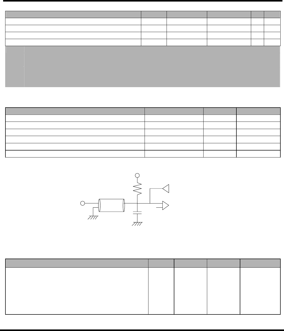
Output load condition
VIL(AC) VREF - 0.31
See Load Circuit
V
Input Differential Voltage, CK and /CK inputs VID(AC) 0.7 VDDQ + 0.6
INPUT / OUTPUT CAPACITANCE
(VDD = 2.6V, VDDQ = 2.6V, TA = 25°C, f = 1MHz)
Parameter
V 1
Max
Input Crossing Point Voltage, CK and /CK inputs VIX(AC) 0.5*VDDQ - 0.2
Unit
Input capacitance (A0~A12, BA0~BA1, /RAS, /CAS, /WE)
0.5*VDDQ + 0.2 V 2
Input capacitance (CKE0)
Input capacitance (/CS0)
Input capacitance (CK0~CK2)
Input capacitance (DM0~DM7)
1. VID is the magnitude of the difference between the input level on CK and the input on /CK. Note:
Data and DQS input/output capacitance (DQ0~DQ63)
C
IN1
CIN2
2. The value of VIX is expected to equal 0.5*V DDQ of the transmitting device and must track variations in the
DC level of the same.
C
IN3
C
IN4
CIN5
3. These parameters should be tested at the pin on actual components and may be checked at either the pin or
the pad in simulation. The AC and DC input specifications are relative to a VREF envelope that has been
bandwidth limited 20MHz.
C
OUT1
65
42
42
AC OPERATING TEST CONDITIONS
(VDD=2.6, VDDQ=2.6, TA=0 to 70°C)
Parameter
28
10
10
Value Unit Note
81
50
50
Input reference voltage for Clock 0.5*VDDQ
34
12
12
pF
V
Input signal maximum peak swing
pF
pF
pF
1.5 V
pF
pF
ZO=50ohm
VTT=0.5*VDDQ
RT=50ohm
C
LOAD
=30pF
Output
Output Load circuit
VREF
=0.5*VDDQ
Symbol Min