
Data Sheet

14
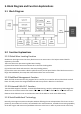
4. Pin Assignments
4.1 Serial ATA Interface Connector
4.2 Pin Assignments
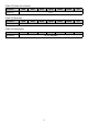
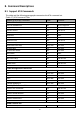
[Table 16] Pin Assignments
Word. No. Plug Connector Pin Definition
Signal
S1 GND
1)
2
nd
mate / Ground
S2 A +
Differential Signal A from Phy
S3 A -
S4 GND
1)
2
nd
mate / Ground
S5 B -
Differential Signal B from Phy
S6 B +
S7 GND
1)
2
nd
mate / Ground
Power
P1 NC
4)
P2 NC
4)
P3 DEVSLP
3)
Device Activity Signal
P4 GND
1)
1
st
mate / Ground
P5 GND
1)
2
nd
mate / Ground
P6 GND
1)
2
nd
mate / Ground
P7 5V 5V Power
P8 5V 5V Power
P9 5V 5V Power
P10 GND
1)
2
nd
mate / Ground
P11 DAS
2)
Device Activity Signal
P12 GND
1)
1
st
mate / Ground
P13 NC
4)
P14 NC
4)
P15 NC
4)
Note:
1) For SATA 2.5 inch SSD, these pins are connected to GND internally.
2) Device Activity Signal / Disable Staggered Spin-up
3) Device Sleep is an input pin. If driven high, the host is informing the SSD to enter a low power state.
4) NC means the SSD does not connect to these pins internally.