
Datasheet
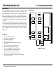


TS32MLS64V6G
168PIN PC133 Unbuffered DIMM
256MB With 16Mx16 CL3
Transcend information Inc.
5
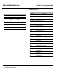
ABSOLUTE MAXIMUM RATINGS
Parameter Symbol Value Unit
Voltage on any pin relative to Vss VIN, VOUT -1.0~4.6 V
Voltage on VDD supply relative to Vss VDD, VDDQ -1.0~4.6 V
Storage temperature TSTG -55~+150
°C
Power dissipation PD 8 W
Short circuit current LOS 50 mA
Operating Temperature TA 0~70
°C
Note: Permanent device damage may occur if ABSOLUTE MAXIMUM RATINGS are exceeded.
Functional operation should be restricted to recommended operating condition.
Exposure to higher than recommended voltage for extended periods of time could affect device reliability.
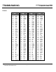
DC OPERATING CONDITIONS AND CHARACTERISTICS
Recommended operating conditions (Voltage referenced to Vss = 0V, TA = 0 to 70 °C)
Parameter Symbol Min Typ Max Unit Note
Supply voltage VDD 3.0 3.3 3.6 V
Input high voltage VIH 2.0 3.0 VDD+0.3 V 1
Input low voltage VIL -0.3 0 0.8 V 2
Output high voltage VOH 2.4 - - V IOH = -2mA
Output low voltage VOL - - 0.4 V IOL = 2mA
Input leakage current ILI -10 - 10 uA 3
Note:
1. VIH (max) = 5.6V AC. The overshoot voltage duration is < 3ns.
2. VIL (min) = -2.0V AC. The undershoot voltage duration is < 3ns.
3. Any input 0V ≤ Vin ≤VDDQ.
Input leakage currents include Hi-Z output leakage for all bi-directional buffers with Tri-state output.
CAPACITANCE (VDD = 3.3V, TA = 23℃, f = 1MHz, VREF = 1.4V ± 200mV)
Parameter Symbol Min Max Unit
Input capacitance (A0~A12, BA0~BA1)
Input capacitance (/RAS, /CAS, /WE)
Input capacitance (CKE0, CKE1)
Input capacitance (CLK0~CLK3)
Input capacitance (/CS0~/CS3)
Input capacitance (DQM0~DQM7)
Data input/output capacitance (DQ0~DQ63)
CADD
C
IN
CCKE
CCLK
CCS
CDQM
C
OUT
25
25
15
15
15
10
13
45
45
25
21
25
12
18
pF
pF
pF
pF
pF
pF
pF
DC CHARACTERISTICS
(Recommended operating condition unless otherwise noted, TA = 0 to 70°C)
Parameter Symbol Test Condition Value Unit Note