
Datasheet

T
T
T
S
S
S
2
2
2
5
5
5
6
6
6
M
M
M
F
F
F
B
B
B
7
7
7
2
2
2
V
V
V
8
8
8
U
U
U
-
-
-
T
T
T
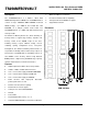
240PIN DDR2 800 Fully Buffered DIMM
2GB With 128Mx8 CL5
Transcend Information Inc.
2
Dimensions
Side Millimeters Inches
A 133.35±0.15 5.250±0.006
B 51 2.0
C 67 2.64
D 5 0.197
E 2.5 0.0980
F 1.5±0.10 0.059±0.039
G 5.175 0.204
H 3.25 0.128
I 3 0.118
J 9.5 0.374
K 18.8 0.74
L 30.35±0.15 1.2±0.006
M 1.27±0.10 0.050±0.004
N 6.80 0.268
(Refer Placement)
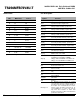
Pin Description
Symbol Function
SCK System Clock Input, positive line
/SCK System Clock Input, negative line
PN[13:0] Primary Northbound Data, positive lines
/PN[13:0] Primary Northbound Data, negative lines
PS[9:0] Primary Southbound Data, positive lines
/PS[9:0] Primary Southbound Data, negative lines
SN[13:0] Secondary Northbound Data, positive lines
/SN[13:0] Secondary Northbound Data, negative lines
SS[9:0] Secondary Southbound Data, positive lines
/SS[9:0] Secondary Southbound Data, negative lines
SCL Serial Presence Detect (SPD) Clock Input
SDA SPD Data Input / Output
SA[2:0]
SPD Address Input, also used to select the
DIMM number in the AMB
VID[1:0]
Voltage ID: these pins must be unconnected
for DDR2-base Fully Buffered DIMMs
VID[0] is VDD value:OPEN=1.8V,GND=1.5V
VID[1] is Vcc value:OPEN=1.5V,GND=1.2V
RESET AMB reset signal
RFU Reserved for Future Use
VCC
AMB Core Power and AMB Channel interface
Power (1.5 Volt)
VDD
DRAM Power and AMB DRAM I/O Power (1.8
Volt)
VTT
DRAM Address/Command/Clock Termination
Power (VDD/2)
VDDSPD SPD Power
VSS Ground
DNU/M_Test
The DNU/M Test pin provides an external
connection R/Cs A-D for testing the margin of
Vref which is produced by a voltage divider on
the module. It is not intended to be used in
normal system operation and must not be
connected(DNU) in a system. This test pin
may have other features on future card
designs and if it does, will be included in this
specification at that time.