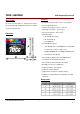
TTS S22G G~~1166G GC CFF330000 300X CompactFlash Card Features Description The Transcend CF 300X is a High Speed Compact • CompactFlash Specification Version 4.1 Complaint Flash Card with high quality Flash Memory assembled • RoHS compliant products • Single Power Supply: 3.3V±5% or 5V±10% on a printed circuit board.
TTS S22G G~~1166G GC CFF330000 300X CompactFlash Card Transcend Transcend Information Inc. 2 V1.
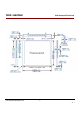
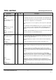
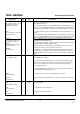
TTS S22G G~~1166G GC CFF330000 300X CompactFlash Card Block Diagram Transcend Information Inc. 3 V1.
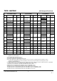
TTS S22G G~~1166G GC CFF330000 300X CompactFlash Card Pin Assignments and Pin Type PC Card Memory Mode Pin Num Signal Name 1 GND 2 D03 3 Pin Type PC Card I/O Mode In, Out Type Pin Num Signal Name Ground 1 GND I/O I1Z, OZ3 2 D03 D04 I/O I1Z, OZ3 3 4 D05 I/O I1Z, OZ3 5 D06 I/O 6 D07 7 -CE1 Pin Type True IDE Mode4 In, Out Type Pin Num Signal Name Ground 1 GND I/O I1Z, OZ3 2 D03 I/O I1Z, OZ3 D04 I/O I1Z, OZ3 3 D04 I/O I1Z, OZ3 4 D05 I/O I1Z, OZ3 4 D05
TTS S22G G~~1166G GC CFF330000 300X CompactFlash Card PC Card Memory Mode Pin Num Signal Name 34 -IORD 10 HSTROBE HDMARDY11 35 -IOWR STOP Pin Type PC Card I/O Mode In, Out Type I I3U I 10,11 I3U Pin Num Signal Name 34 -IORD 10 HSTROBE -HDMARDY11 35 -IOWR STOP Pin Type In, Out Type Pin Num Signal Name 34 -IORD HSTROBE8 9 -HDMARDY Pin Type In, Out Type I I3Z I I3Z 7 I I 10,11 True IDE Mode4 I3U I3U 35 -IOWR STOP 7 8,9 36 -WE I I3U 36 -WE I I3U 36 -WE3 I I
TTS S22G G~~1166G GC CFF330000 300X CompactFlash Card Signal Description Signal Name A10 – A00 Dir. I (PC Card Memory Mode) Pin Description 8,10,11,12, These address lines along with the -REG signal are used to select the following: 14,15,16,17, The I/O port address registers within the CompactFlash Storage Card , the memory mapped port address registers within the CompactFlash Storage Card, 18,19,20 a byte in the card's information structure and its configuration control and status registers.
TTS S22G G~~1166G GC CFF330000 Signal Name -CE1, -CE2 300X CompactFlash Card Dir. Pin I 7,32 (PC Card Memory Mode) Card Enable Description These input signals are used both to select the card and to indicate to the card whether a byte or a word operation is being performed. -CE2 always accesses the odd byte of the word.-CE1 accesses the even byte or the Odd byte of the word depending on A0 and -CE2. A multiplexing scheme based on A0,-CE1, -CE2 allows 8 bit hosts to access all data on D0-D7.
TTS S22G G~~1166G GC CFF330000 Signal Name -INPACK 300X CompactFlash Card Dir. Pin O 43 Description This signal is not used in this mode. (PC Card Memory Mode except Ultra DMA Protocol Active) The Input Acknowledge signal is asserted by the CompactFlash Storage Card when the card is selected and responding to an I/O read cycle at the address that is on the address bus. This signal is used by the host to control the enable of any input data buffers between the CompactFlash Storage Card and the CPU.
TTS S22G G~~1166G GC CFF330000 Signal Name -IOWR (PC Card Memory Mode– Except Ultra DMA Protocol Active) 300X CompactFlash Card Dir. Pin I 35 Description This signal is not used in this mode. The I/O Write strobe pulse is used to clock I/O data on the Card Data bus into the CompactFlash Storage Card controller registers when the CompactFlash Storage Card is configured to use the I/O interface.
TTS S22G G~~1166G GC CFF330000 Signal Name -REG 300X CompactFlash Card Dir. Pin I 44 (PC Card Memory Mode– Except Ultra DMA Protocol Active) Description This signal is used during Memory Cycles to distinguish between Common Memory and Register (Attribute) Memory accesses. High for Common Memory, Low for Attribute Memory.
TTS S22G G~~1166G GC CFF330000 Signal Name -VS1 -VS2 300X CompactFlash Card Dir. Pin O 33 40 (PC Card Memory Mode) -VS1 -VS2 Description Voltage Sense Signals. -VS1 is grounded on the Card and sensed by the Host so that the CompactFlash Storage Card CIS can be read at 3.3 volts and -VS2 is reserved by PCMCIA for a secondary voltage and is not connected on the Card. This signal is the same for all modes. (PC Card I/O Mode) -VS1 -VS2 This signal is the same for all modes.
TTS S22G G~~1166G GC CFF330000 300X CompactFlash Card Electrical Specification The following tables indicate all D.C. Characteristics for the CompactFlash Storage Card. Unless otherwise stated, conditions are: Vcc = 5V ±10% Vcc = 3.3V ± 5% Absolute Maximum Conditions DC Characteristics CompactFlash Interface I/O at 5.0V Parameter Symbol Min. Max. Unit Supply Voltage High level output voltage Low level output voltage VCC VOH VOL 4.5 5.5 0.8 1.
TTS S22G G~~1166G GC CFF330000 300X CompactFlash Card Input Power Input Leakage Current Input Characteristics for UDMA mode >4 In UDMA modes greater than 4, the following characteristics apply. Voltage output high and low values shall be met at the source connector to include the effect of series termination.
TTS S22G G~~1166G GC CFF330000 300X CompactFlash Card Output Drive Characteristics for UDMA mode > 4 In UDMA modes greater than 4, the characteristics specified in the following table apply. Voltage output high and low values shall be met at the source connector to include the effect of series termination. Table: Output Drive Characteristics (UDMA Mode > 4) Parameter Symbol MIN MAX Units DC supply voltage to drivers VDD3 3.3 –8% 3.
TTS S22G G~~1166G GC CFF330000 Item Control Signal Signal -CE1 -CE2 -REG -IORD -IOWR -OE -WE RESET Status Signal 300X CompactFlash Card 10 Card Host 10 Pull-up to VCC 500 KΩ ≧ R≧ 50 KΩ and shall be sufficient to keep inputs inactive when the pins are not connected at the 1 host. Pull-up to VCC 500 KΩ ≧ R ≧ 50 KΩ . Pull-up to VCC 500 KΩ ≧ R ≧ 50 KΩ . READY -WAIT WP 1,2 1,2,9, Pull-up to VCC R ≧ 10 KΩ . 3 In PCMCIA PC Card modes Pull-up to VCC 4 R ≧ 10 KΩ .
TTS S22G G~~1166G GC CFF330000 300X CompactFlash Card Notes: 1) Control Signals: each card shall present a load to the socket no larger than 50 pF 10 at a DC current of 700 μ A low state and 150 μ A high state, including pull-resistor. The socket shall be able to drive at least the following load 10 while meeting all AC timing requirements: (the number of sockets wired in parallel) multiplied by (50 pF with DC current 700 μ A low state and 150 μ A high state per socket). 2) Resistor is optional.
TTS S22G G~~1166G GC CFF330000 300X CompactFlash Card 4) The -WAIT and IORDY signals shall be ignored by the host. Devices supporting CF Advanced timing modes shall also support slower timing modes, to ensure operability with systems that do not support CF Advanced timing modes Transcend Information Inc. 17 V1.
TTS S22G G~~1166G GC CFF330000 300X CompactFlash Card Ultra DMA Electrical Requirements Host and Card signal capacitance limits for Ultra DMA operation The host interface signal capacitance at the host connector shall be a maximum of 25 pF for each signal as measured at 1 MHz. The card interface signal capacitance at the card connector shall be a maximum of 20 pF for each signal as measured at 1 MHz.
TTS S22G G~~1166G GC CFF330000 300X CompactFlash Card Table: Ultra DMA Termination with Pull-up or Pull down Example Printed Circuit Board (PCB) Trace Requirements for Ultra DMA On any PCB for a host or device supporting Ultra DMA: The longest D[15:00] trace shall be no more than 0.5" longer than either STROBE trace as measured from the IC pin to the connector. The shortest D[15:00] trace shall be no more than 0.5" shorter than either STROBE trace as measured from the IC pin to the connector.
TTS S22G G~~1166G GC CFF330000 300X CompactFlash Card Attribute Memory Read Timing Specification Attribute Memory access time is defined as 300 ns.
TTS S22G G~~1166G GC CFF330000 300X CompactFlash Card Configuration Register (Attribute Memory) Write Timing Specification The Card Configuration write access time is defined as 250 ns. Detailed timing specifications are shown in Table below.
TTS S22G G~~1166G GC CFF330000 300X CompactFlash Card Common Memory Read Timing Specification Cycle Time Mode: 250 ns 100 ns 80 ns Ma x ns.
TTS S22G G~~1166G GC CFF330000 300X CompactFlash Card Common Memory Write Timing Specification Cycle Time Mode: 250 ns 120 ns Max ns. Min ns. Max ns. 100 ns Min ns. Max ns. 80 ns Min ns. Item Symbol IEEE Symbol Min ns.
TTS S22G G~~1166G GC CFF330000 300X CompactFlash Card I/O Input (Read) Timing Specification Cycle Time Mode: Item Symbol IEEE Symbol 250 ns Min ns. 120 ns Max ns. Min ns. Max ns. Min ns. Max ns. Min ns.
TTS S22G G~~1166G GC CFF330000 300X CompactFlash Card I/O Output (Write) Timing Specification Cycle Time Mode: Item Symbol IEEE Symbol 255 ns Min ns. Max ns. 120 ns Min ns. Max ns. 100 ns Min ns. Max ns. 80 ns Min ns.
TTS S22G G~~1166G GC CFF330000 300X CompactFlash Card True IDE PIO Mode Read/Write Timing Specification Mode Item 0 1 Note 2 3 4 5 6 t0 Cycle time (min) 600 383 240 180 120 100 80 t1 Address Valid to -IORD/-IOWR setup (min) 70 50 30 30 25 15 10 t2 -IORD/-IOWR (min) 165 125 100 80 70 65 55 1 t2 -IORD/-IOWR (min) Register (8 bit) 290 290 290 80 70 65 55 1 t2i -IORD/-IOWR recovery time (min) - - - 70 25 25 20 1 t3 -IOWR data setup (min) 60 45 30
TTS S22G G~~1166G GC CFF330000 Transcend Information Inc. 300X CompactFlash Card 27 V1.
TTS S22G G~~1166G GC CFF330000 300X CompactFlash Card True IDE Multiword DMA Mode Read/Write Timing Specification The timing diagram for True IDE DMA mode of operation in this section is drawn using the conventions in the ATA-4 specification. Signals are shown with their asserted state as high regardless of whether the signal is actually negative or positive true. Consequently, the -IORD, the -IOWR and the -IOCS16 signals are shown in the diagram inverted from their electrical states on the bus.
TTS S22G G~~1166G GC CFF330000 300X CompactFlash Card True IDE Ultra DMA Mode Read/Write Timing Specification Ultra DMA operations can take place in any of the three basic interface modes: PC Card Memory mode, PC Card I/O mode, and True IDE (the original mode to support UDMA).
TTS S22G G~~1166G GC CFF330000 300X CompactFlash Card select the Ultra DMA mode at which the system operates. The Ultra DMA mode selected by a host shall be less than or equal to the fastest mode of which the device is capable. Only one Ultra DMA mode shall be selected at any given time. All timing requirements for a selected Ultra DMA mode shall be satisfied. Devices supporting any Ultra DMA mode shall also support all slower Ultra DMA modes.
TTS S22G G~~1166G GC CFF330000 Name UDMA Mode 0 Min Max 300X CompactFlash Card UDMA Mode 1 Min Max UDMA Mode 2 Min Max UDMA Mode 3 Min Max UDMA Mode 4 Min Max UDMA Mode 5 Min Measure location (see Note 2) Max t2CYCTYP 240 160 120 90 60 40 Sender tCYC 112 73 54 39 25 16.8 Note 3 t2CYC 230 153 115 86 57 38 Sender tDS 15.0 10.0 7.0 7.0 5.0 4.0 Recipient tDH 5.0 5.0 5.0 5.0 5.0 4.6 Recipient tDVS 70.0 48.0 31.0 20.0 6.7 4.8 Sender tDVH 6.2 6.2 6.
TTS S22G G~~1166G GC CFF330000 300X CompactFlash Card incoming transition from the recipient or sender respectively. Both the incoming signal and the outgoing response shall be measured at the same connector. 5) The parameter tAZ shall be measured at the connector of the sender or recipient that is driving the bus but must release the bus the allow for a bus turnaround.
TTS S22G G~~1166G GC CFF330000 300X CompactFlash Card Notes: 1) The parameters tUI, tMLI : (Ultra DMA Data-In Burst Device Termination Timing and Ultra DMA Data-In Burst Host Termination Timing), and tLI indicate sender-to-recipient or recipient-to-sender interlocks, i.e., one agent (either sender or recipient) is waiting for the other agent to respond with a signal before proceeding. tUI is an unlimited interlock that has no maximum time value. tMLI is a limited time-out that has a defined minimum.
TTS S22G G~~1166G GC CFF330000 Name Comment SRISE SFALL 300X CompactFlash Card Min [V/ns] Max [V/ns] Notes Rising Edge Slew Rate for any signal 1.25 1 Falling Edge Slew Rate for any signal 1.25 1 Note: 1) The sender shall be tested while driving an 18 inch long, 80 conductor cable with PVC insulation material. The signal under test shall be cut at a test point so that it has not trace, cable or recipient loading after the test point.
TTS S22G G~~1166G GC CFF330000 300X CompactFlash Card Card Configuration The CompactFlash Storage Cards is identified by appropriate information in the Card Information Structure (CIS). The following configuration registers are used to coordinate the I/O spaces and the Interrupt level of cards that are located in the system.
TTS S22G G~~1166G GC CFF330000 300X CompactFlash Card Table: PC Card Memory Mode UDMA Function -DMACK -REG STOP -IOW R -DMARDY -IORD (R)-WAIT (W) STROBE -WAIT (R)-IORD (W) DMA CMD A10A00 -CE2 -CE1 -DMARQ -INPACK 1 1 1 X X X X No XX Standby X X 0 1 X X 1 YES XX Device UDMA Transfer Request (Assert DMARQ) X X 0 1 1 X 1 YES XX Host Acknowledge Preparation 1 1 0 1 1 1 1 YES Static Host Acknowledge Preparation 1 1 0 0 1 1 1 YES Static DMA Acknowledge (S
TTS S22G G~~1166G GC CFF330000 300X CompactFlash Card Attribute Memory Function Attribute memory is a space where CompactFlash Storage Card identification and configuration information are stored, and is limited to 8 bit wide accesses only at even addresses. The card configuration registers are also located here. For CompactFlash Storage Cards, the base address of the Card configuration registers is 200h.
TTS S22G G~~1166G GC CFF330000 300X CompactFlash Card Configuration Option Register (Base + 00h in Attribute Memory) Transcend Information Inc. 38 V1.
TTS S22G G~~1166G GC CFF330000 300X CompactFlash Card Card Configuration and Status Register (Base + 02h in Attribute Memory) Transcend Information Inc. 39 V1.
TTS S22G G~~1166G GC CFF330000 300X CompactFlash Card Pin Replacement Register (Base + 04h in Attribute Memory) Transcend Information Inc. 40 V1.
TTS S22G G~~1166G GC CFF330000 300X CompactFlash Card Socket and Copy Register (Base + 06h in Attribute Memory) Transcend Information Inc. 41 V1.
TTS S22G G~~1166G GC CFF330000 300X CompactFlash Card I/O Transfer Function The I/O transfer to or from the CompactFlash Storage can be either 8 or 16 bits. When a 16 bit accessible port is addressed, the signal -IOIS16 is asserted by the CompactFlash Storage. Otherwise, the -IOIS16 signal is de-asserted. When a 16 bit transfer is attempted, and the -IOIS16 signal is not asserted by the CompactFlash Storage, the system shall generate a pair of 8 bit references to access the word‘s even byte and odd byte.
TTS S22G G~~1166G GC CFF330000 300X CompactFlash Card Table: PC Card I/O Mode UDMA Function DMACK -REG STOP -IOWR -DMARDY -IORD (R)-WAIT (W) STROBE -WAIT (R)-IORD (W) DMA CMD A10A00 -CE2 -CE1 -DMARQ -INPACK 1 1 1 X X X X No XX Standby X X 0 0 X X 1 YES XX Device UDMA Transfer Request (Assert DMARQ) X X 0 0 1 X 1 YES XX Host Acknowledge Preparation 1 1 0 0 1 1 1 YES Static Host Acknowledge Preparation 1 1 0 1 1 1 1 YES Static DMA Acknowledge (Stoppe
TTS S22G G~~1166G GC CFF330000 300X CompactFlash Card Common Memory Transfer Function The Common Memory transfer to or from the CompactFlash Storage can be either 8 or 16 bits.
TTS S22G G~~1166G GC CFF330000 300X CompactFlash Card True IDE Mode I/O Transfer Function The CompactFlash Storage Card can be configured in a True IDE Mode of operation. The CompactFlash Storage Card is configured in this mode only when the -OE input signal is grounded by the host during the power off to power on cycle. Optionally, CompactFlash Storage Cards may support the following optional detection methods: 1.
TTS S22G G~~1166G GC CFF330000 300X CompactFlash Card Host Configuration Requirements for Master/Slave or New Timing Modes The CF Advanced Timing modes include PCMCIA PC Card style I/O modes that are faster than the original 250 ns cycle time. These modes are not supported by the PCMCIA PC Card specification nor CF by cards based on revisions of the CF specification before Revision 3.0.
TTS S22G G~~1166G GC CFF330000 300X CompactFlash Card CF-ATA Drive Register Set Definition and Protocol The CompactFlash Storage Card can be configured as a high performance I/O device through: a) The standard PC-AT disk I/O address spaces 1F0h-1F7h, 3F6h-3F7h (primary) or 170h- 177h, 376h-377h (secondary) with IRQ 14 (or other available IRQ). b) Any system decoded 16 byte I/O block using any available IRQ. c) Memory space.
TTS S22G G~~1166G GC CFF330000 300X CompactFlash Card I/O Primary and Secondary Address Configurations Table: Primary and Secondary I/O Decoding Transcend Information Inc. 48 V1.
TTS S22G G~~1166G GC CFF330000 300X CompactFlash Card Contiguous I/O Mapped Addressing When the system decodes a contiguous block of I/O registers to select the CompactFlash Storage Card, the registers are accessed in the block of I/O space decoded by the system as follows: Table: Contiguous I/O Decoding Transcend Information Inc. 49 V1.
TTS S22G G~~1166G GC CFF330000 300X CompactFlash Card Memory Mapped Addressing When the CompactFlash Storage Card registers are accessed via memory references, the registers appear in the common memory space window: 0-2K bytes as follows: True IDE Mode Addressing When the CompactFlash Storage Card is configured in the True IDE Mode, the I/O decoding is as follows: Transcend Information Inc. 50 V1.
TTS S22G G~~1166G GC CFF330000 300X CompactFlash Card CF-ATA Registers The following section describes the hardware registers used by the host software to issue commands to the CompactFlash device. These registers are often collectively referred to as the “task file.” Data Register (Address - 1F0h[170h];Offset 0,8,9) The Data Register is a 16 bit register, and it is used to transfer data blocks between the CompactFlash Storage Card data buffer and the Host. This register overlaps the Error Register.
TTS S22G G~~1166G GC CFF330000 300X CompactFlash Card Feature Register (Address - 1F1h[171h]; Offset 1, 0Dh Write Only) This register provides information regarding features of the CompactFlash Storage Card that the host can utilize. This register is also accessed in PC Card modes on data bits D15-D8 during a write operation to Offset 0 with -CE2 low and -CE1 high.
TTS S22G G~~1166G GC CFF330000 300X CompactFlash Card Bit 3 (HS3): when operating in the Cylinder, Head, Sector mode, this is bit 3 of the head number. It is Bit 27 in the Logical Block Address mode. Bit 2 (HS2): when operating in the Cylinder, Head, Sector mode, this is bit 2 of the head number. It is Bit 26 in the Logical Block Address mode. Bit 1 (HS1): when operating in the Cylinder, Head, Sector mode, this is bit 1 of the head number. It is Bit 25 in the Logical Block Address mode.
TTS S22G G~~1166G GC CFF330000 300X CompactFlash Card Device Control Register (Address - 3F6h[376h]; Offset Eh) This register is used to control the CompactFlash Storage Card interrupt request and to issue an ATA soft reset to the card. This register can be written even if the device is BUSY. The bits are defined as follows: Bit 7: this bit is ignored by the CompactFlash Storage Card. The host software should set this bit to 0. Bit 6: this bit is ignored by the CompactFlash Storage Card.
TTS S22G G~~1166G GC CFF330000 300X CompactFlash Card Card (Drive) Address Register (Address 3F7h[377h]; Offset Fh) This register is provided for compatibility with the AT disk drive interface. It is recommended that this register not be mapped into the host’s I/O space because of potential conflicts on Bit 7. Bit 7: this bit is unknown.
TTS S22G G~~1166G GC CFF330000 300X CompactFlash Card CF-ATA Command Set CF-ATA Command Set summarizes the CF-ATA command set with the paragraphs that follow describing the individual commands and the task file for each.
TTS S22G G~~1166G GC CFF330000 300X CompactFlash Card 29 Set Feature EFh Y – – – Y – Support 30 Set Multiple Mode C6h – Y – – Y – Support 31 Set Sleep Mode E6h or 99h – – – – Y – Support 32 Standby E2 or 96h – – – – Y – Support 33 Standby Immediate E0 or 94h – – – – Y – Support 34 Translate Sector 87h – Y Y Y Y Y Support 35 Wear Level F5h – – – – Y – Support 36 Write Buffer E8h – – – – Y – Support 37 Write DMA CAh – Y Y
TTS S22G G~~1166G GC CFF330000 300X CompactFlash Card Check Power Mode - 98h or E5h If the CompactFlash Storage Card is in, going to, or recovering from the sleep mode, the CompactFlash Storage Card sets BSY, sets the Sector Count Register to 00h, clears BSY and generates an interrupt. If the CompactFlash Storage Card is in Idle mode, the CompactFlash Storage Card sets BSY, sets the Sector Count Register to FFh, clears BSY and generates an interrupt.
TTS S22G G~~1166G GC CFF330000 300X CompactFlash Card Erase Sector(s) - C0h This command is used to pre-erase and condition data sectors in advance of a Write without Erase or Write Multiple without Erase command. There is no data transfer associated with this command but a Write Fault error status can occur.
TTS S22G G~~1166G GC CFF330000 300X CompactFlash Card Identify Device – Ech Bit -> 7 6 5 4 Command (7) C/D/H (6) 3 2 1 0 ECh X X X Drive X Cyl High (5) X Cyl Low (4) X Sec Num (3) X Sec Cnt (2) X Feature (1) X The Identify Device command enables the host to receive parameter information from the CompactFlash Storage Card. This command has the same protocol as the Read Sector(s) command.
TTS S22G G~~1166G GC CFF330000 300X CompactFlash Card Word Address Default Value Total Bytes 51 0X00h 2 PIO data transfer cycle timing mode 52 0000h 2 Obsolete 53 000Xh 2 Field Validity 54 XXXXh 2 Current numbers of cylinders 55 XXXXh 2 Current numbers of heads 56 XXXXh 2 Current sectors per track 57-58 XXXXh 4 Current capacity in sectors (LBAs)(Word 57 = LSW, Word 58 = MSW) 59 01XXh 2 Multiple sector setting 60-61 XXXXh 4 Total number of sectors addressable in LBA Mo
TTS S22G G~~1166G GC CFF330000 300X CompactFlash Card Word 0: General Configuration This field indicates the general characteristics of the device. When Word 0 of the Identify drive information is 848Ah then the device is a CompactFlash Storage Card and complies with the CFA specification and CFA command set. It is recommended that PCMCIA modes of operation report only the 848Ah value as they are always intended as removable devices. Bits 15-0: CF Standard Configuration Value Word 0 is 848Ah.
TTS S22G G~~1166G GC CFF330000 300X CompactFlash Card Words 7-8: Number of Sectors per Card This field contains the number of sectors per CompactFlash Storage Card. This double word value is also the first invalid address in LBA translation mode. Words 10-19: Serial Number This field contains the serial number for this CompactFlash Storage Card and is right justified and padded with spaces (20h).
TTS S22G G~~1166G GC CFF330000 300X CompactFlash Card Multiple Sector Setting Bits 15-9 are reserved and shall be set to 0. Bit 8 shall be set to 1 indicating that the Multiple Sector Setting is valid. Bits 7-0 are the current setting for the number of sectors that shall be transferred per interrupt on Read/Write Multiple commands. Total Sectors Addressable in LBA Mode This field contains the total number of user addressable sectors for the CompactFlash Storage Card in LBA mode only.
TTS S22G G~~1166G GC CFF330000 300X CompactFlash Card If this field is supported, bit 1 of word 53 shall be set to one. The value in word 66 shall not be less than the value in word 65. This field shall be supported by all CompactFlash Storage Cards supporting DMA modes 1 and above. If bit 1 of word 53 is set to one, but this field is not supported, the Card shall return a value of zero in this field.
TTS S22G G~~1166G GC CFF330000 300X CompactFlash Card If bit 3 of word 83 is set to one, the CompactFlash Storage Card supports the Advanced Power Management feature set. Bit 4 of word 83 shall be set to zero; the CompactFlash Storage Card does not support the Removable Media Status feature set. Words 85-87: Features/command sets enabled Words 85, 86, and 87 shall indicate features/command sets enabled.
TTS S22G G~~1166G GC CFF330000 Bit 5: Bit 4: Bit 3: Bit 2: Bit 1: Bit 0: 1 = Ultra DMA mode 5 and below are supported. Bits 0-4 Shall be set to 1. 1 = Ultra DMA mode 4 and below are supported. Bits 0-3 Shall be set to 1. 1 = Ultra DMA mode 3 and below are supported, Bits 0-2 Shall be set to 1. 1 = Ultra DMA mode 2 and below are supported. Bits 0-1 Shall be set to 1. 1 = Ultra DMA mode 1 and below are supported. Bit 0 Shall be set to 1.
TTS S22G G~~1166G GC CFF330000 300X CompactFlash Card Bit 13: -XP If set to 1, indicates that the CompactFlash Storage Card does not have Power Level 1 commands. If set to 0, indicates that the CompactFlash Storage Card has Power Level 1 commands Bit 12: -XE If set to 1, indicates that Power Level 1 commands are disabled. If set to 0, indicates that Power Level 1 commands are enabled. Bit 0-11: Maximum current This field contains the CompactFlash Storage Card’s maximum current in mA.
TTS S22G G~~1166G GC CFF330000 2 3-7 300X CompactFlash Card PIO Mode 6 Reserved Bits 11-9: Advanced True IDE Multiword DMA Mode Selected Indicates the current True IDE Multiword DMA Mode Selected on the card. Value Current Multiword DMA timing mode selected 0 Specified in word 63 1 Multiword DMA Mode 3 2 Multiword DMA Mode 4 3-7 Reserved Bits 15-12 are reserved.
TTS S22G G~~1166G GC CFF330000 300X CompactFlash Card 2 3 4 5 6 7 PC Card I/O UDMA mode 2 supported PC Card I/O UDMA mode 3 supported PC Card I/O UDMA mode 4 supported PC Card I/O UDMA mode 5 supported Reserved Reserved Bits 11-9: Maximum PC Card Memory UDMA timing mode supported Indicates the Maximum PC Card Memory UDMA timing mode supported by the card when bit 15 is set.
TTS S22G G~~1166G GC CFF330000 300X CompactFlash Card Command (7) 97h or E3h C/D/H (6) X Drive X Cyl High (5) X Cyl Low (4) X Sec Num (3) X Sec Cnt (2) Timer Count (5 msec increments) Feature (1) X Idle Immediate - 95h or E1h This command causes the CompactFlash Storage Card to set BSY, enter the Idle mode, clear BSY and generate an interrupt.
TTS S22G G~~1166G GC CFF330000 300X CompactFlash Card Cyl High (5) X Cyl Low (4) X Sec Num (3) X Sec Cnt (2) X Feature (1) X Read Buffer - E4h The Read Buffer command enables the host to read the current contents of the CompactFlash Storage Card’s sector buffer. This command has the same protocol as the Read Sector(s) command.
TTS S22G G~~1166G GC CFF330000 Read Multiple - C4h Read Sector(s) - 20h or 21h Read Verify Sector(s) - 40h or 41h Recalibrate - 1Xh Transcend Information Inc. 300X CompactFlash Card 73 V1.
TTS S22G G~~1166G GC CFF330000 300X CompactFlash Card Request Sense - 03h The extended error code is returned to the host in the Error Register. Seek - 7Xh Transcend Information Inc. 74 V1.
TTS S22G G~~1166G GC CFF330000 300X CompactFlash Card Set Features – EFh Feature Supported Features 01h and 81h are used to enable and clear 8 bit data transfer modes in True IDE Mode. If the 01h feature command is issued all data transfers shall occur on the low order D[7:0] data bus and the -IOIS16 signal shall not be asserted for data register accesses. The host shall not enable this feature for DMA transfers.
TTS S22G G~~1166G GC CFF330000 300X CompactFlash Card Feature 03h allows the host to select the PIO or Multiword DMA transfer mode by specifying a value in the Sector Count register. The upper 5 bits define the type of transfer and the low order 3 bits encode the mode value. One PIO mode shall be selected at all times. For Cards which support DMA, one Multiword DMA mode shall be selected at all times. The host may change the selected modes by the Set Features command.
TTS S22G G~~1166G GC CFF330000 Standby Immediate - 94h or E0h Translate Sector - 87h 300X CompactFlash Card Translate Sector Information Transcend Information Inc. 77 V1.
TTS S22G G~~1166G GC CFF330000 Wear Level - F5h Write Buffer - E8h Write DMA – CAh Transcend Information Inc. 300X CompactFlash Card 78 V1.
TTS S22G G~~1166G GC CFF330000 Write Long Sector - 32h or 33h Write Multiple Command - C5h Write Multiple without Erase – CDh Transcend Information Inc. 300X CompactFlash Card 79 V1.
TTS S22G G~~1166G GC CFF330000 Write Sector(s) - 30h or 31h Write Sector(s) without Erase - 38h Write Verify - 3Ch Transcend Information Inc. 300X CompactFlash Card 80 V1.
TTS S22G G~~1166G GC CFF330000 300X CompactFlash Card Error Posting Command Error Register BBK UNC IDNF Check Power Mode Status Register ABRT AMNF V Execute Drive Diagnostic1 Erase Sector(s) DRDY DWF DSC V V V V V V V V V Flush Cache V V V Format Track V V V CORR ERR V V V V V V V V V V V V Identify Device V V V V V Idle V V V V V Idle Immediate V V V V V V V V Initialize Drive Parameters Key Management Structure Read V V V V V V Key
TTS S22G G~~1166G GC CFF330000 300X CompactFlash Card Command Error Register BBK UNC IDNF Status Register ABRT AMNF DRDY DWF DSC CORR ERR Set Multiple Mode V V V V V Set Sleep Mode V V V V V Stand By V V V V V Stand By Immediate V V V V V Translate Sector V Wear Level V V V V V V V V V V V V V V V V V V V V Write Buffer V Write DMA V V V V V V V V Write Long Sector V V V V V V V V Write Multiple V V V V V V V V Write M
TTS S22G G~~1166G GC CFF330000 300X CompactFlash Card SMART Data Structure BYTE Decription F/V 0-1 X Revision code 2-361 X Vendor specific 362 V Off line data collection status 363 X Self-test execution status byte 364-365 V Total time in seconds to complete off-line data collection activity 366 X Vendor specific 367 F Off-line data collection capability 368-369 F SMART capability Error logging capability 370 F 7-1 Reserved 0 1=Device error logging supported 371 X Vendor