
upduino-readthedocs-io-en-latest


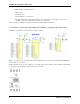
Table Of Contents

UPduino Documentation, Release 0.1
• open fpga verilog tutorial.
Tools
• Icarus Verilog.
• GTKWave.
• Verilator.
UPduino Examples
• XarkLabs SystemVerilog Example <https://github.com/XarkLabs/upduino-example> - demonstrates simulation
and other aspects of a more complete software toolchain
1.1.5 Specifications
The UPduino supports the following features:
• Lattice iCE40 UP5K UG48 FPGA
UPduino Pinout
The UPduino pinout was kindly provided by Xark below.
• G0/G1/G3/G6 refer to Global clock inputs.
• gpio_20 is used for the on-board 12MHz oscillator if the OSC jumper is shorted.
• gpio_35 is the ideal location to supply a clock as this will allow placement of the PLL right next to it.
• If gpio_35 is used as an input, y nything other than a clock, you cannot use a PLL in your design!
• qSPI flash access is possible by shorting the jumpers on the board: note that this uses up gpio_10 and
gpio_20.
PCF Pin# _____ Pin# PCF
------| USB |------
<GND> | 1 \___/ 48 | spi_ssn (16)
<VIO> | 2 47 | spi_sck (15)
<RST> | 3 46 | spi_mosi (17)
<DONE> | 4 45 | spi_miso (14)
<RGB2> led_red | 5 44 | gpio_20 <N/A w/OSC, G3>
<RGB0> led_green | 6 U 43 | gpio_10
<RGB1> led_blue | 7 P 42 | <GND>
<+5V> | 8 D 41 | <12 MHz>
<+3.3V> | 9 U 40 | gpio_12
<GND> | 10 I 39 | gpio_21
gpio_23 | 11 N 38 | gpio_13
gpio_25 | 12 O 37 | gpio_19
gpio_26 | 13 36 | gpio_18
gpio_27 | 14 V 35 | gpio_11
gpio_32 | 15 3 34 | gpio_9
<G0> gpio_35 | 16 . 33 | gpio_6
gpio_31 | 17 0 32 | gpio_44 <G6>
<G1> gpio_37 | 18 31 | gpio_4
(continues on next page)
4 Chapter 1. tinyVision.ai