
upduino-readthedocs-io-en-latest
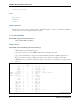
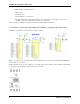
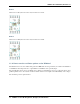
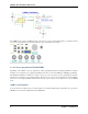
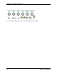
Table Of Contents

UPduino Documentation, Release 0.1
Bank 0:
Cut the trace for R31 (shorted on the board) and solder across R19.
Bank 2:
Cut the trace for R20 (shorted on the board) and solder across R26.
1.1.9 How to use the oscillator options on the UPduino?
The UPduino has an on-board oscillator that generates 12MHz. This clock is generated by an oscillator and distributed
to the FTDI, an external pin and also to a global buffer on the FPGA via an optional jumper.
The pin IOB_25B_G3 was chosen specifically as it is already in a bank thats forced to be at 3.3V levels. If any other
global capable IO were to be used, this would force that IO bank to not be capable of the full flexibility of IO voltages.
The schematic portion is captured below:
1.1. UPDuino v3.0: PCB Design Files, Designs, Documentation 7