
Users Manual Part 2
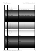
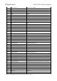
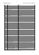
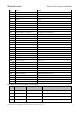
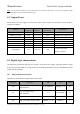
Table Of Contents
- 1 Physical Description
- 2 Interfaces Description
- 2.1 Interfaces Parameter Definitions
- 2.2 Interfaces Detail Description
- 2.2.1 Power Supply Interface
- 2.2.2 Touchscreen Interface
- 2.2.3 Display Interface
- 2.2.4 Camera Interfaces
- 2.2.5 Audio Interface
- 2.2.6 USB & DisplayPort Interface
- 2.2.7 PCIe Interface
- 2.2.8 SSC Interface
- 2.2.9 SDIO Interface
- 2.2.10 QUP Interface
- 2.2.11 Power on Interface
- 2.2.12 Reset Interface
- 2.2.13 Keys Interface
- 2.2.14 Sensor Interrupt Interface
- 2.2.15 Debug UART Interface
- 2.2.16 Battery Interface
- 2.2.17 ADCs Interface
- 2.2.18 PWMs and LED Current Driver Interface
- 2.2.19 Antenna Interface
- 3 Connector PIN Summary
- 4 Electrical Characteristics

Thundercomm TurboX C865 System on Module
Copyright © 2018 All Rights Reserved, Thundercomm Technology Co., Ltd.
3
G38
6DOF_2V8_EN
GPIO 84
G39
6DOF_1V8_EN
GPIO 83
G40
GPIO_22_C
GPIO 22
G41
GPIO_23
GPIO 23
G42
CAM1_RST_N
Camera 1 reset, GPIO 92
G43
SD_UFS_CARD_DET_N
SD CARD detection, GPIO 77
G44
GPIO_144_C
GPIO 144
G45 WSA_SWR_DATA Audio PA sound wire data
G46 WSA_SWR_CLK Audio PA sound wire clock
G47
VBATT_CONN_VSENSE_M
Battery current sense minus
G48
GND
GND
G49
GND
GND
G50
GND
GND
H1
NC
NC
H2
NC
NC
H3
NC
NC
H4
NC
NC
H5
NC
NC
H6 NC NC
H7 NC NC
H8
NC
NC
H9
NC
NC
H10
NC
NC
H11
CSI0_A0_CLK_M
MIPI CSI 0 (DPHY), differential clock – minus
H12
GND
GND
H13
CSI0_A1_LN1_P
MIPI CSI 0 (DPHY), differential lane 1 – plus
H14
GND
GND
H15 CSI0_C1_LN2_P MIPI CSI 0 (DPHY), differential lane 2 – plus
H16 GND GND
H17 DSI0_C1_CLK_M MIPI DSI 0 (DPHY), differential clock – minus
H18
GND
GND
H19
DSI0_B2_LN2_M
MIPI DSI 0 (DPHY), differential lane 2 – minus
H20
GND
GND
H21
PCIE2_REFCLK_P_MDM
PCIe 2 Gen3 reference clock - plus
H22
GND
GND
H23
PCIE2_RX0_P_MDM
PCIe 2 Gen 3 receive 0 - plus
H24
GND
GND
H25 PCIE2_TX1_P_MDM PCIe 2 Gen 3 transmit 1 - plus
H26 GPIO_31 GPIO 31
H27
GPIO_30
GPIO 30
H28
GPIO_29
GPIO 29
H29
GPIO_28
GPIO 28
H30
GPIO_6
GPIO 6