
Users Manual Part 2
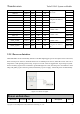
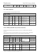
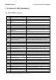
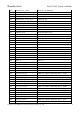
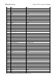
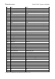
Table Of Contents
- 1 Physical Description
- 2 Interfaces Description
- 2.1 Interfaces Parameter Definitions
- 2.2 Interfaces Detail Description
- 2.2.1 Power Supply Interface
- 2.2.2 Touchscreen Interface
- 2.2.3 Display Interface
- 2.2.4 Camera Interfaces
- 2.2.5 Audio Interface
- 2.2.6 USB & DisplayPort Interface
- 2.2.7 PCIe Interface
- 2.2.8 SSC Interface
- 2.2.9 SDIO Interface
- 2.2.10 QUP Interface
- 2.2.11 Power on Interface
- 2.2.12 Reset Interface
- 2.2.13 Keys Interface
- 2.2.14 Sensor Interrupt Interface
- 2.2.15 Debug UART Interface
- 2.2.16 Battery Interface
- 2.2.17 ADCs Interface
- 2.2.18 PWMs and LED Current Driver Interface
- 2.2.19 Antenna Interface
- 3 Connector PIN Summary
- 4 Electrical Characteristics

Thundercomm TurboX C865 System on Module
Copyright © 2018 All Rights Reserved, Thundercomm Technology Co., Ltd.
2
C23
GND
GND
C24
DSI1_B2_LN2_M
MIPI DSI 1 (DPHY), differential lane 2 – minus
C25
GND
GND
C26
DSI1_B0_LN0_M
MIPI DSI 1 (DPHY), differential lane 0 – minus
C27
GND
GND
C28
DSI1_NC_LN3_M
MIPI DSI 1 (DPHY), differential lane 3 – minus
C29
GND
GND
C30 USB0_SS_RX1_M USB super-speed 0 receive 1 – minus
C31 GND GND
C32
USB0_SS_TX0_M
USB super-speed 0 transmit 0 – minus
C33
GND
GND
C34
DP_AUX_N
AUX N for DP
C35
GND
GND
C36
FP_SPI_CS
SPI selection
C37
FP_SPI_MISO
SPI MISO
C38
FSA_INT_N
GPIO 63
C39
GPIO_10_P
GPIO 10
C40
GPIO_88
GPIO 88
C41 GPIO_89 GPIO 89
C42 GPIO_54 GPIO 54
C43
SDM_FORCE_USB_BOOT
Force boot configuration
C44
6DOF_R_RS
GPIO
C45
SDM_DEBUG_UART_RX
Uart RX for system debug
C46
WCD_RESET_N
SoundWire reset
C47
GND
GND
C48
GND
GND
C49
GND
GND
C50 GND GND
D1 NC NC
D2 GND GND
D3
RF_CH1_CON
WiFi 2.4/5G RF out, Chain1
D4
GND
GND
D5
SDM_WDOG_DISABLE
GPIO 128
D6
NC
NC
D7
GPIO_137
GPIO 137
D8
NC
NC
D9
NC
NC
D10 NC NC
D11 PCIE1_RX0_M PCIe 1 Gen 3 receive 0 – minus
D12
GND
GND
D13
PCIE1_REFCLK_M
PCIe 1 Gen 3 reference clock – minus
D14
GND
GND
D15
PCIE1_TX0_M
PCIe 1 Gen 3 transmit 0 – minus