
Users Manual Part 2
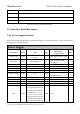
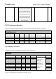
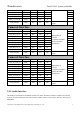
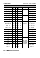
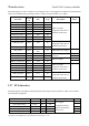
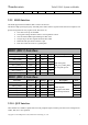
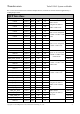
Table Of Contents
- 1 Physical Description
- 2 Interfaces Description
- 2.1 Interfaces Parameter Definitions
- 2.2 Interfaces Detail Description
- 2.2.1 Power Supply Interface
- 2.2.2 Touchscreen Interface
- 2.2.3 Display Interface
- 2.2.4 Camera Interfaces
- 2.2.5 Audio Interface
- 2.2.6 USB & DisplayPort Interface
- 2.2.7 PCIe Interface
- 2.2.8 SSC Interface
- 2.2.9 SDIO Interface
- 2.2.10 QUP Interface
- 2.2.11 Power on Interface
- 2.2.12 Reset Interface
- 2.2.13 Keys Interface
- 2.2.14 Sensor Interrupt Interface
- 2.2.15 Debug UART Interface
- 2.2.16 Battery Interface
- 2.2.17 ADCs Interface
- 2.2.18 PWMs and LED Current Driver Interface
- 2.2.19 Antenna Interface
- 3 Connector PIN Summary
- 4 Electrical Characteristics

Thundercomm TurboX C865 System on Module
Copyright © 2018 All Rights Reserved, Thundercomm Technology Co., Ltd.
1
2.2.8 SSC Interface
The SOM has an integrated sensor subsystem called Snapdragon™ sensor core (SSC), which is dedicated to
support low-power, always-on use cases.
The sensor subsystem can be left powered on even when the rest of the MSM device is in sleep mode. The
SSC has a dedicated 1.5MB L2/TCM cache.
The SSC core has dedicated I/O to communicate with the sensors. The I/O scan support I2C and SPI
interfaces.
SSC Interface
PIN Name
Location
PIN
Voltage
Type
Description
Notes
SNS_I2C0_SDA CON1 J37
P3
IO
These I2C signals are
dedicated to Sensor
GPIO160
SNS_I2C0_SCL CON1 H37
P3
IO GPIO161
SNS_I2C4_SDA CON1 H38
P3
IO
These I2C signals are
dedicated to Sensor
GPIO170
SNS_I2C4_SCL CON1 H39
P3
IO GPIO171
SPI2_MISO_IMU CON1 J40
P3
IO
Snapdragon™ Sensor
Core SPI signals
GPIO164
SPI2_MOSI_IMU CON1 J41
P3
IO GPIO165
SPI2_CLK_IMU CON1 J38
P3
IO GPIO166
PCIE1_RX1_P
CON1
F12
AI
PCIE1_TX0_M
CON1
D15
AO
PCIE1_TX0_P CON1 E15 AO
PCIE1_TX1_M CON1 E14 AO
PCIE1_TX1_P CON1 F14 AO
GPIO_83
CON1
G39
DI
PCIE Clock request
GPIO_82
CON1
G37
DO
PCIe reset signal
GPIO_84
CON1
G38
DI
PCIe wake up signal
PCIE2_REFCLK_M_MDM
CON1
J21
AO
PCIe Signals
Compliant with PCI
Express Specification
Revision 3.0
PCIE2_REFCLK_P_MDM
CON1
H21
AO
PCIE2_RX0_M_MDM
CON1
J23
AI
PCIE2_RX0_P_MDM
CON1
H23
AI
PCIE2_RX1_M_MDM CON1 K22 AI
PCIE2_RX1_P_MDM CON1 J22 AI
PCIE2_TX0_M_MDM
CON1
K24
AI
PCIE2_TX0_P_MDM
CON1
J24
AI
PCIE2_TX1_M_MDM
CON1
J25
AO
PCIE2_TX1_P_MDM
CON1
H25
AO
GPIO_86
CON1
D39
DI
PCIe clock require
GPIO_85
CON1
F39
DO
PCIe reset signal
Table 2.2-4 PCIe interface definition