
User's Manual Part 2

Exciter Configuration Description - 61 -
®
Affinity LBD-200C-N1 Transmitter
Product Manual
The synthesizer sub-module design combines Direct Digital Synthesizer (DDS), and Phase
Lock Loop (PLL) technology to allow for wideband, low resolution, and low phase noise
performance. Combining a DDS with a PLL in an RF synthesizer allows frequency resolution
and controllability of the DDS while maintaining the frequency range of the PLL system. The
PLL can reduce DDS spurious, whereas the DDS can decrease PLL multiplication factor,
enhancing phase noise performance of the overall system. Together they provide for a high
performance RF synthesizer. This design is a modified translation loop approach containing
three phase locked loops, however its core operation depends on a single main loop with an
embedded direct digital synthesizer, allowing a simpler overall architecture as compared to
traditional multi loop synthesizers, a design method previously hard to achieve without the use
of a custom ASIC or complex multistage architecture. The highly integrated direct digital
synthesizer incorporates many of the design stages necessary for the translation loop approach
such as integrated PLL and mixer stages. Proprietary circuits and techniques allowing wideband
operation with fine step size resolution are applied.
To maintain frequency stability the synthesizer requires a reference frequency. Two options are
offered in this design, a 10MHz external reference and/or an internal reference. In the internal
reference, a PLL system locks an on-board voltage controlled Oven Controlled Crystal Oscillator
(OCXO) to the incoming reference input allowing the external reference to control the internal
reference while present, and allows minimal system impact in the event that the external
reference is lost. The internal reference oscillator circuitry will sense the presence of the
external source and select this source as the primary frequency stability determining input. In
the event that the external reference is absent, the synthesizer will automatically substitute a
voltage on the OCXO V-tune input. This methodology is more complex and costly but adds
reliability to SFN transmission systems by allowing a phase continuous input to the synthesizer.
Usually, the external reference frequency is a signal that is obtained from a GPS or Loran C
broadcast. These navigational broadcasts frequencies are driven from a master reference
oscillator that is traceable to a NIST level-1 frequency clock. The external reference enters the
module through an RF female coaxial contact of the DIN41612-M connector. The input is
matched using a resistive load for 50-ohm impedance. An output of the PLL processed internal
reference is also offered on a separate RF female coaxial contact of the DIN41612-M
connector. The incoming signal is sampled and detected by a logarithmic amplifier detector.
This information, in the form of an analog DC voltage proportional to the signal level, is sent to
the MCU for diagnostics. An LED present on the front panel indicates reference status. The
reference signal is limited so that the level at the input connector can be as high as +30dBm
with no damage to the input circuitry, however, a nominal level of +5dBm is recommended and
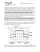
a level above -5dBm should always be maintained. Note that the phase noise of the reference
will affect phase noise performance of the LO outputs. The main Phase Lock Loop (PLL) uses a
wide loop bandwidth, and reference noise is one of the dominating factors determining phase
noise at close offsets to the carrier below the loop filter cutoff. The client should exercise caution
when selecting the reference source if the internal OCXO option is not installed. In order to
minimize cost impacts, the high stability internal OCXO reference will remain an option that the
client must request at time of order. The 10MHz signal also forms the reference input to the
1000MHz PLO.