
User's Manual Part 2
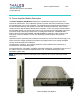

Power Amplifier Module - 110 -
®
Affinity LBD-200C-N1 Transmitter
Product Manual
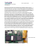
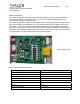
Microcontroller Board
Control and monitoring functions of the PA Module segment is accomplished through the
Microcontroller Board located within the PA Module segment housing. The Microcontroller
Board uses an 8-bit microcontroller unit (MCU) with on-board memory to perform the control
and monitoring functions. The microcontroller board includes analog signal conditioning, A/D
and D/A converters, supply voltage regulation, and serial data interfaces.
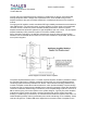
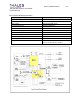
Monitoring operations involve collecting analog signals and logic data from the power amplifier
segments. Analog inputs, forward power, reflected power, and temperature, are received from
the RF power amp connector J1. The analog input drain supply voltage (V
DD), and high voltage
DC is received from power supply connector J2. Forward power and reflected power inputs are
amplified by operational amplifiers with a gain of approximately two, while temperature, drain
supply voltage, and high voltage DC is buffered by unity gain stages. Following the V
DD buffer
stage, a resistor divider network scales V
DD to ¼ of the input voltage followed by a second unity
gain buffering stage. Each of these inputs is voltage-limited to 5.1 V
DC by means of Zener
diodes at the input to the microcontroller board.
The Microcontroller Board monitors drain current drawn by Field Effect Transistors (FET) in the
RF power amplifier section of the PA Module. The microcontroller achieves this by monitoring
the voltages dropped across series resistors in the drain supply circuits on the power supply
board. The control board from the power supply connector J2 receives these eight voltages.
Each signal is selected by the MCU, and related CPLD logic, through an eight-channel analog
multiplexer (MUX) IC, and in turn compared to VDD by a differential amp/gain op-amp stage.
The resulting outputs are 10-times greater than the voltages dropped across the series
monitoring resistors. These outputs are protected from voltages greater than 5.1V
DC by Zener
diodes and from voltages more negative than –0.4 V
DC by Schottky diodes. The resulting signal
is connected to input AN0/IDSMON on the MCU A/D converter. This signal varies through time
with each of the eight monitored signals as selected by the MCU.
The control board provides various logic inputs and outputs. A drain supply enable signal,
PS_ENABLE, is outputted from the microcontroller board on J2. The state of PS_ENABLE is
controlled by the MCU, which tests other signals such as Standby, Maximum drain currents,
V
DD voltage, and temperature of the heat sink to determine if it is safe to enable the power
supply. The MCU outputs the Enable Signal to the CPLD, which in turn outputs the
OS_ENABLE on J2. If the MCU detects a condition unsafe to allow the drain supply to operate,
the CPLD will output a logic-LOW on the PS_ENABLE control output.
Output signals that control the RF power amplifier attenuator, and the Phase Shifter, are
generated on the control board. Signal RF_ATTEN_CTRL1 and Phase Shifter are analog
outputs that control the branches of the RF attenuator and RF Phase Shifter network located in
the RF amplifier section. These analog voltages are developed in a D/A converter IC, NPN,
PNP, and MOSFET transistors. The serial input/output (I/O) capabilities of the Power Amplifier
Segment originate on the control board and the MCU SCI port.
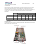
In general, the Power Amplifier segment may be connected to an RS-485 multidrop network as
an individually addressed node with other amplifier segments. Node address switch SW1 is a
DIP multi-pole switch that is programmed with a PA segment’s unique node address in binary
form. While present on the network, a PA Module may be issued specific commands from, and
return formatted responses to, a master communication device. By default the RS-485 driver IC
is enabled. The RS-485 serial I/O is available on J3 of the backplane connector. An RS-232