
User's Manual Part 2

Driver Section - 80 -
®
Affinity LBD-200C-N1 Transmitter
Product Manual
supply section, the output voltage will shut down when commanded by the microcontroller. The
output of this power supply section is only used to power the remote interface circuitry on the
user interface module in the exciter.
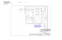
+8V
DC: A linear regulator provides the +8VDC from the +12VDC power supply section. This
regulator is filtered to clean any AC component coupled across/induced from the regulator.
Diodes protect the regulator from over-voltage and reverse-voltage load conditions. A resetable
fuse further protects the regulator during overload conditions. Since the positive voltage enabled
switch controls the supply voltage to this power supply section, the output voltage will shutdown
when commanded by the microcontroller. The output of this power supply section is only used
within other sections of the Driver.
+5V
DC: A linear regulator provides a +5VDC output from the +12VDC power supply section. This
power is used with the Power Supply Plug-in for powering the digital monitoring circuits of the
power supply plug-in, and the Master Control Interface (MSI). To assure continuous operation of
the controlling circuitry, this voltage is not controlled by the positive voltage enable.
-12V
DC: A switching power supply converts voltage from the +12VDC supply to approximately –
16V
DC. This voltage level is filtered and regulated to -12VDC. Diodes protect the regulator from
reverse and over-voltage load conditions. The output of this power supply is fused to prevent
damage to the power supply circuit during transitional overloads.
Similar to the +12V
DC power supply section, a negative voltage enabled switch controls the
application of -12V
DC to the remaining plug-ins within the Driver.
Power Supply Enable: The positive and negative power supplies work identically, with the
exception of the direction of current flow and type of MOSFET transistor switching the power to
the system. TTL logic from the embedded controller is applied to NPN transistors that supply
sufficient current to drive optocouplers.
The optocouplers have a Darlington-pair transistor drive that when enabled, create a current
draw from the supply voltage, across two resistors, through the optocoupler and ground. This
current draw across the resistors provides a voltage drop.
A tie-point in between the resistors takes the difference in potential to the gate of the transistor.
The difference of potential between the source and drain causes the MOSFET to conduct,
turning on the voltage to the rest of the circuitry behind the switch.
When there is no current flow across the resistors (when the optocoupler is not conducting),
there is no current flow through the resistors, no voltage drop across the resistors, and the
potential from the gate to source remains the same. The MOSFET will not conduct and will
switch off the power to the remaining circuitry behind the transistor.
Current and Voltage monitoring: Current sampling is accomplished by measuring the voltage
drop across a resistor in series with the load. The voltages from both sides of the resistor are
scaled down in order to keep the measured voltages from the supply voltages of the operational
amplifiers. The voltage differences are buffered and applied to an operational amplifier
configured to measure the difference of the two input voltages.
The output of the differential amplifier is applied to a non-inverting amplifier to increase the
voltage near the middle of the system controller 5-volt analog-to-digital converter range. An
integrated circuit containing Zener and Shottkey diodes protect the inputs of the system
controller. The system controller compares this value against previously calibrated values to
determine if the power supply is operating outside of specified parameters.