
User's Manual
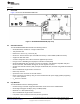
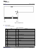

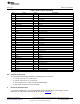


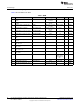
Table Of Contents

www.ti.com
Board Pin Assignment
Figure 3 shows the bottom view of the EVB.
Figure 3. EVB (Bottom View)
2.1 Pin Description
Table 1 describes the board pins.
Table 1. Pin Description
No. Name Type Description
1 SLOW_CLK I Slow clock input option (default: NU)
2 GND G Ground
3 GND G Ground
4 WL_EN I WLAN enable
5 V
BAT
P 3.6-V typical voltage input
6 GND G Ground
7 V
BAT
P 3.6-V typical voltage input
8 V
IO
P V
IO
1.8-V (I/O voltage) input
9 GND G Ground
10 N.C. No connection
11 WL_RS232_TX O WLAN tool RS232 output
12 N.C. No connection
13 WL_RS232_RX I WLAN tool RS232 input
14 N.C. No connection
15 WL_UART_DBG O WLAN Logger output
16 N.C. No connection
17 N.C. No connection
18 GND G Ground
19 GND G Ground
20 SDIO_CLK I WLAN SDIO clock
5
SWRU382–November 2014 WL1837MODCOM8I WLAN MIMO and Bluetooth
®
Module Evaluation Board for
TI Sitara™ Platform
Submit Documentation Feedback
Copyright © 2014, Texas Instruments Incorporated