
User's Manual
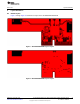
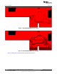


Table Of Contents

Layout Guidelines
www.ti.com
Figure 13 shows the trace design for the PCB. TI recommends using a 50-Ω impedance match on the
trace to the antenna and 50-Ω traces for the PCB layout.
Figure 13. Trace Design for the PCB Layout
Figure 14 shows layer 1 with the trace to the antenna over ground layer 2.
Figure 14. Layer 1 Combined With Layer 2
Figure 15 and Figure 16 show instances of good layout practices for the antenna and RF trace routing.
NOTE: RF traces must be as short as possible. The antenna, RF traces, and modules must be on
the edge of the PCB product. The proximity of the antenna to the enclosure and the
enclosure material must also be considered.
14
WL1837MODCOM8I WLAN MIMO and Bluetooth
®
Module Evaluation Board SWRU382–November 2014
for TI Sitara™ Platform
Submit Documentation Feedback
Copyright © 2014, Texas Instruments Incorporated