
User Guide
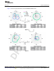
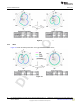
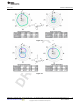

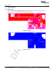
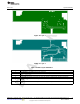
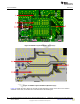
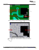
Table Of Contents

Layout Guidelines
www.ti.com
Figure 18. Module Layout Guidelines (Top Layer)
Figure 19. Module Layout Guidelines (Bottom Layer)
Figure 20 shows the trace design for the PCB. A 50-Ω impedance match on the trace to the antenna
should be used. Also, 50-Ω traces are recommended for the PCB layout.
18
WL1835MODCOM8A WLAN MIMO and BT Module Evaluation Board for TI SWRU359A–September 2013–Revised October 2013
Sitara™ Platform
Submit Documentation Feedback
Copyright © 2013, Texas Instruments Incorporated