WL1835MODCOM8A WLAN MIMO and BT Module Evaluation Board for TI Sitara™ Platform User's Guide Literature Number: SWRU359A September 2013 – Revised October 2013
Contents Preface ....................................................................................................................................... 3 1 Introduction ........................................................................................................................ 4 2 3 4 5 6 7 2 .................................................................................................................. 4 ...................................................................................
Preface SWRU359A – September 2013 – Revised October 2013 Read This First About This Manual This user's guide describes how to use the TI WL1835MODCOM8A board to evaluate the performance of the TI WL1835MODGA module. Related Documentation From Texas Instruments • • TI WiLink8 Single-Band Combo Module – Wi-Fi, BT, and BLE (SWRS152) WiLink 8 Wiki: http://www.ti.com/wilink8wiki If You Need Assistance The primary sources of WL1835MODGA information are the device-specific data sheets and user’s guides.
User's Guide SWRU359A – September 2013 – Revised October 2013 WL1835MODCOM8A WLAN MIMO and BT Module Evaluation Board for TI Sitara™ Platform 1 Introduction The WL1835MODCOM8A device is a WiFi® MIMO, Bluetooth®, and Bluetooth Low Energy (BLE) module board with the TI WL1835MODGA module. WL1835MODGA is built-in TI WL1835 IEEE 802.11 b/g/n and Bluetooth 4.0 solutions to provide the best WiFi and Bluetooth coexistence interoperability and powersaving technologies from TI. Figure 1.
Introduction www.ti.com 1.2 Applications • • • • • • • 1.3 Internet of Things Multimedia Home Electronics Home Appliances and White Goods Industrial and Home Automation Smart Gateway and Metering Video Conferencing Video Camera and Security TI Module Key Benefits • • • • • • • • Reduces Design Overhead: Single WiLink8™ Module Scales Across Wi-Fi and Bluetooth. WLAN High Throughput: 80 Mbps (TCP), 100 Mbps (UDP) Bluetooth 4.
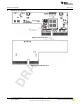
Board Pin Assignment 2 www.ti.com Board Pin Assignment Figure 2. Board Top View Figure 3.
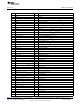
Board Pin Assignment www.ti.com 2.1 Pin Descriptions No. Name Type Description 1 SLOW_CLK I Slow clock input 2 GND G Ground 3 GND G Ground 4 WL_EN I WLAN Enable 5 VBAT P Power supply input 6 GND G Ground 7 VBAT P Power supply input 8 VIO P Power supply input for I/O pin 9 GND G Ground 10 N.C. 11 WL_RS232_TX 12 N.C. 13 WL_RS232_RX 14 N.C. 15 WL_UART_DBG 16 N.C. 17 N.C. 18 GND G Ground 19 GND G Ground 20 SDIO_CLK I WLAN SDIO clock 21 N.C.
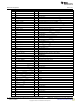
Board Pin Assignment 8 www.ti.com No. Name Type 48 N.C. No connection 49 N.C. No connection 50 N.C. No connection 51 N.C. No connection 52 PCM_IF_CLK 53 N.C. 54 PCM_IF_FSYNC 55 N.C. 56 PCM_IF_DIN 57 N.C. 58 PCM_IF_DOUT 59 N.C. 60 GND 61 N.C. 62 N.C. 63 GND G Ground 64 GND G Ground 65 N.C. 66 BT_UART_IF_TX 67 N.C. 68 BT_UART_IF_RX 69 N.C. 70 BT_UART_IF_CTS 71 N.C. 72 BT_UART_IF_RTS 73 N.C. 74 BT_FUNC1 75 N.C.
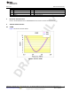
Electrical Characteristics www.ti.com 3 No. Name Type Description 97 GND G Ground 98 GPIO12 I/O General-purpose I/O 99 N.C. 100 GPIO10 General-purpose I/O I/O General-purpose I/O Electrical Characteristics Refer to the detailed data in the WL1835MODGA data sheet for electrical characteristics. 4 Antenna Characteristics 4.1 VSWR Figure 4 shows the antenna VSWR. Figure 4.
Antenna Characteristics 4.2 www.ti.com Efficiency Figure 5 shows the antenna efficiency. Figure 5. Antenna Efficiency 5 Antenna Characteristics 5.1 Radio Pattern Figure 6 shows the radio pattern of the WL1835MODCOM8A device. Figure 6.
Antenna Characteristics www.ti.com 5.1.1 ANT1 Figure 7 shows the ANT1 polarization of the WL1835MODCOM8A device. Figure 7. Figure 8.
Antenna Characteristics www.ti.com Figure 9. 5.1.2 ANT2 Figure 10 shows the ANT2 polarization of the WL1835MODCOM8A device. Figure 10.
Antenna Characteristics www.ti.com Figure 11. Figure 12.
Circuit Design www.ti.com 6.1 Schematic WLAN_EN_SOC R1 0R 0402 BT_EN_SOC R2 0R 0402 WL_UART_DBG R4 0R 0402 BT_UART_DBG TP8 R3 J1 HEADER 1x2 H-1X2_2MM 2 1 Circuit Design TP2 1 TP1 1 VIO_IN 0R 0402 1 VBAT_IN C2 10uF 0603 R32 0R 0402 C1 1uF 0402 R31 0R 0402 C3 0.1uF 0402 SLOW_CLK R5 OSC1 1V8 / 32.768kHz VIO_IN OSC-3.2X2.5 3 1 OUT EN SLOW_CLK R6 0R 0402 2 1 6 2 GND VCC 4 VBAT_IN C4 0.
Circuit Design www.ti.com 6.2 Bill of Materials (BOM) Table 1 lists the bill of materials. Table 1. BOM 1 TI WL1835 WiFi/Bluetooth Module WL1835MODGA U1 2 XOSC 3225 / 32.768 kHz / 1.8 V / ±50 ppm 7XZ3200005 OSC1 3 ANT / Chip / 2.4 GHz, 5 GHz / Peak Gain >5 dBi ANT016008LCD2442MA1 ANT1, ANT2 4 CON Male 1x2 / Pitch P301-SGP-040/028-02 J1, J3, J4 5 DC JUMPER / PITCH 2.0 mm CMJ-20BB J1, J3 6 Mini RF Header Receptacle U.FL-R-SMT-1(10) J5, J6 7 IND 0402 / 1.1 nH / ±0.
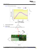
Layout Guidelines 7 Layout Guidelines 7.1 Board Layout www.ti.com Figure 14 shows the WL1835MODCOM8A 4-layer board. Table 2, Figure 15, Figure 16, Figure 17, Figure 18, and Figure 19 show instances of good layout practices. Figure 14. Layer 1 Figure 15.
Layout Guidelines www.ti.com Figure 16. Layer 3 Figure 17. Layer 4 Table 2. Module Layout Guidelines Reference Guideline Description 1 The proximity of ground vias must be close to the pad. 2 Signal traces must not be run underneath the module on the layer where the module is mounted. 3 Have a complete ground pour in layer 2 for thermal dissipation. 4 Have a solid ground plane and ground vias under the module for stable system and thermal dissipation.
Layout Guidelines www.ti.com Figure 18. Module Layout Guidelines (Top Layer) Figure 19. Module Layout Guidelines (Bottom Layer) Figure 20 shows the trace design for the PCB. A 50-Ω impedance match on the trace to the antenna should be used. Also, 50-Ω traces are recommended for the PCB layout.
Layout Guidelines www.ti.com Figure 20. Trace Design for the PCB Layout Figure 21 shows layer 1 with the trace to the antenna over ground layer 2. Figure 21. Layer 1 Combined With Layer 2 Table 3, Figure 22, and Figure 23 describe instances of good layout practices for the antenna and RF trace routing. Table 3. Antenna and RF Trace Routing Layout Guidelines Reference Guideline Description 1 The RF trace antenna feed must be as short as possible beyond the ground reference.
Layout Guidelines www.ti.com Figure 22. Top Layer – Antenna and RF Trace Routing Layout Guidelines Figure 23.
Layout Guidelines www.ti.com Figure 24 describes the MIMO antenna spacing. The distance of ANT1 and ANT2 must be greater than half of wavelength (62.5 mm @ 2.4 GHz). Figure 24. MIMO Antenna Spacing The supply routing guidelines are as follows: • For power supply routing, the power trace for VBAT must be at least 40 mil wide. • The 1.8-V trace must be at least 18 mil wide. • Make VBAT traces as wide as possible to ensure reduced inductance and trace resistance.
Revision History www.ti.com This user's guide revision history highlights the technical changes made to the SWRU359 device-specific user's guide. Revision History Revision Date SWRS359A October 2013 Description / Changes Changed all references of the device name from WL1835MODCOM8 to WL1835MODCOM8A. NOTE: Page numbers for previous revisions may differ from page numbers in the current version.