
Datasheet


"#$%&'
SBAS417B − JUNE 2007 − REVISED JANUARY 2008
www.ti.com
4
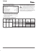
ELECTRICAL CHARACTERISTICS: V
S
= +2.7V to +5.5V (continued)
At T
A
= −40°C to +85°C, +V
CC
= +2.7V, V
REF
= 2.5V internal voltage, f
SAMPLE
= 125kHz, f
CLK
= 16 • f
SAMPLE
= 2MHz, 12-bit mode, digital
inputs = GND or IOVDD, and +V
CC
must be ≥ IOVDD, unless otherwise noted.
TSC2046E
PARAMETER UNITSMAXTYPMINCONDITION
DIGITAL INPUT/OUTPUT
Logic Family CMOS
Capacitance All Digital Control Input Pins 5 15 pF
V
IH
| I
IH
| ≤ +5µA IOVDD • 0.7 IOVDD + 0.3 V
V
IL
| I
IL
| ≤ +5µA −0.3 0.3 • IOVDD V
V
OH
I
OH
= −250µA IOVDD • 0.8 V
V
OL
I
OL
= 250µA 0.4 V
Data Format
Straight
Binary
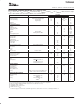
POWER-SUPPLY REQUIREMENTS
+V
CC
(5)
Specified Performance 2.7 3.6 V
Operating Range 2.2 5.25 V
IOVDD
(6)
1.5 +V
CC
V
Quiescent Current
(7)
Internal Reference Off 280 650 µA
Internal Reference On 780 µA
f
SAMPLE
= 12.5kHz 220 µA
Power-Down Mode with 3 µA
CS = DCLK = DIN = IOVDD
Power Dissipation +V
CC
= +2.7V 1.8 mW
TEMPERATURE RANGE
Specified Performance −40 +85 °C
(1)
LSB means Least Significant Bit. With V
REF
= +2.5V, 1 LSB is 610µV.
(2)
Assured by design, but not tested. Exceeding 50mA source current may result in device degradation.
(3)
Difference between TEMP0 and TEMP1 measurement, no calibration necessary.
(4)
Temperature drift is −2.1mV/°C.
(5)
TSC2046E operates down to 2.2V.
(6)
IOVDD must be ≤ (+V
CC
).
(7)
Combined supply current from +V
CC
and IOVDD. Typical values obtained from conversions on AUX input with PD0 = 0.