
Datasheet


"#$%&'
SBAS417B − JUNE 2007 − REVISED JANUARY 2008
www.ti.com
17
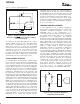
16 Clocks-per-Conversion
The control bits for conversion n + 1 can be overlapped
with conversion n to allow for a conversion every 16 clock
cycles, as shown in Figure 11. This figure also shows
possible serial communication occurring with other serial
peripherals between each byte transfer from the processor
to the converter. (16 clocks cycles are possible, provided
that each conversion completes within 1.6ms of starting.
Otherwise, the signal that is captured on the input
sample-and-hold may droop enough to affect the
conversion result.) Note that the TSC2046E is fully
powered while other serial communications are taking
place during a conversion.
Digital Timing
Figure 9, Figure 12, and Table 6 provide detailed timing for
the digital interface of the TSC2046E.
15 Clocks-per-Conversion
Figure 13 provides the fastest way to clock the
TSC2046E. This method does not work with the serial
interface of most microcontrollers and digital signal
processors, as they are generally not capable of providing
15 clock cycles per serial transfer. However, this method
can be used with field-programmable gate arrays (FPGAs)
or application- specific integrated circuits (ASICs). Note
that this effectively increases the maximum conversion
rate of the converter beyond the values given in the
specification tables, which assume 16 clock cycles per
conversion.
1
DCLK
CS
81
11
DOUT
BUSY
SDIN
Control Bits
S
Control Bits
1098765 43210
11 10 9
81 18
Figure 11. Conversion Timing, 16 Clocks-per-Conversion, 8-Bit Bus Interface.
No DCLK delay required with dedicated serial port
PD0
t
BDV
t
DH
t
CH
t
CL
t
DS
t
CSS
t
DV
t
BD
t
BD
t
TR
t
BTR
t
DO
t
CSH
DCLK
CS
11DOUT
BUSY
DIN
10
Figure 12. Detailed Timing Diagram