
Datasheet


"#$%&'
SBAS417B − JUNE 2007 − REVISED JANUARY 2008
www.ti.com
15
Control Byte
The control byte (on DIN), as shown in Table 3, provides
the start conversion, addressing, ADC resolution,
configuration, and power-down of the TSC2046E.
Figure 9, Table 3 and Table 4 give detailed information
regarding the order and description of these control bits
within the control byte.
Initiate START—The first bit, the S bit, must always be
high and initiates the start of the control byte. The
TSC2046E ignores inputs on the DIN pin until the start bit
is detected.
Addressing—The next three bits (A2, A1, and A0) select
the active input channel(s) of the input multiplexer (see
Table 1, Table 2, and Figure 2), touch screen drivers, and
the reference inputs.
MODE—The mode bit sets the resolution of the ADC. With
this bit low, the next conversion has 12-bit resolution,
whereas with this bit high, the next conversion has 8-bit
resolution.
SER/DFR
—The SER/DFR bit controls the reference
mode, either single-ended (high) or differential (low). The
differential mode is also referred to as the ratiometric
conversion mode and is preferred for X-Position,
Y-Position, and Pressure-Touch measurements for
optimum performance. The reference is derived from the
voltage at the switch drivers, which is almost the same as
the voltage to the touch screen. In this case, a reference
voltage is not needed as the reference voltage to the ADC
is the voltage across the touch screen. In the single-ended
mode, the converter reference voltage is always the
difference between the V
REF
and GND pins (see Table 1
and Table 2, and Figure 2 through Figure 5, for further
information).
BIT 7
(MSB)
BIT 6 BIT 5 BIT 4 BIT 3 BIT 2 BIT 1
BIT 0
(LSB)
S A2 A1 A0 MODE SER/DFR PD1 PD0
Table 3. Order of the Control Bits in the Control
Byte
BIT NAME DESCRIPTION
7 S Start bit. Control byte starts with first high bit on DIN.
A new control byte can start every 15th clock cycle
in 12-bit conversion mode or every 11th clock cycle
in 8-bit conversion mode (see Figure 13).
6-4 A2-A0 Channel Select bits. Along with the SER/DFR bit,
these bits control the setting of the multiplexer input,
touch driver switches, and reference inputs (see
Table 1 and Figure 13).
3 MODE 12-Bit/8-Bit Conversion Select bit. This bit controls
the number of bits for the next conversion: 12-bits
(low) or 8-bits (high).
2 SER/DFR Single-Ended/Differential Reference Select bit. Along
with bits A2-A0, this bit controls the setting of the
multiplexer input, touch driver switches, and
reference inputs (see Table 1 and Table 2).
1-0 PD1-PD0 Power-Down Mode Select bits. Refer to Table 5 for
details.
Table 4. Descriptions of the Control Bits within
the Control Byte
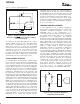
p
t
ACQ
AcquireIdle Conversion Idle
1DCLK
CS
81
11
DOUT
BUSY
Drivers 1 and 2
(1)
(SER/DFR High)
Drivers 1 and 2
(1, 2)
(SER/DFR Low)
(MSB)
(START)
(LSB)
A2S
On
On
Off Off
Off Off
DIN A1 A0 MODE
SER/
DFR
PD1 PD0
1098765 4 3210 ZeroFilled...
81 8
(1) For Y−Position, Driver 1 is on X+ is selected, and Driver 2 is off. For X−Position, Driver 1 is off, Y+ is selected, and Driver 2 is on. Y
−
will turn on
when power−down mode is entered and PD0 = 0.
(2) Drivers will remain on if PD0 = 1 (no power down) until selected input channel, reference mode, or ower−down mode is changed, or CS is high.
NOTES:
Figure 9. Conversion Timing, 24 Clocks-per-Conversion, 8-Bit Bus Interface.
No DCLK delay required with dedicated serial port