
Host Controller Data Manual


2–3
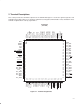
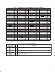
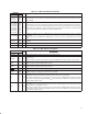
Table 2–2. Signal Names Sorted Alphanumerically to Terminal Number
TERMINAL NAME NO. TERMINAL NAME NO. TERMINAL NAME NO. TERMINAL NAME NO.
CYCLEIN 78 PCI_AD11 59 PCI_CLK 12 PHY_DATA7 81
CYCLEOUT 77 PCI_AD12 58 PCI_CLKRUN 7 PHY_LINKON 98
GND 1 PCI_AD13 57 PCI_DEVSEL 47 PHY_LPS 99
GND 11 PCI_AD14 56 PCI_FRAME 43 PHY_LREQ 97
GND 24 PCI_AD15 54 PCI_GNT 14 PHY_SCLK 95
GND 30 PCI_AD16 40 PCI_IDSEL 29 REG_EN 79
GND 50 PCI_AD17 38 PCI_INTA 8 REG18 42
GND 60 PCI_AD18 37 PCI_IRDY 44 REG18 100
GND 75 PCI_AD19 36 PCI_PAR 52 SCL 4
GND 83 PCI_AD20 34 PCI_PERR 49 SDA 5
GND 94 PCI_AD21 33 PCI_PME 17 V
CCP
6
GPIO2 2 PCI_AD22 32 PCI_REQ 15 V
CCP
16
GPIO3 3 PCI_AD23 31 PCI_RST 76 V
CCP
39
G_RST 10 PCI_AD24 27 PCI_SERR 51 V
CCP
63
PCI_AD0 74 PCI_AD25 26 PCI_STOP 48 V
CCP
87
PCI_AD1 73 PCI_AD26 25 PCI_TRDY 45 3.3 V
CC
9
PCI_AD2 72 PCI_AD27 23 PHY_CTL0 93 3.3 V
CC
13
PCI_AD3 71 PCI_AD28 22 PHY_CTL1 92 3.3 V
CC
20
PCI_AD4 69 PCI_AD29 21 PHY_DATA0 90 3.3 V
CC
35
PCI_AD5 68 PCI_AD30 19 PHY_DATA1 89 3.3 V
CC
46
PCI_AD6 67 PCI_AD31 18 PHY_DATA2 88 3.3 V
CC
55
PCI_AD7 66 PCI_C/BE0 65 PHY_DATA3 86 3.3 V
CC
70
PCI_AD8 64 PCI_C/BE1 53 PHY_DATA4 85 3.3 V
CC
80
PCI_AD9 62 PCI_C/BE2 41 PHY_DATA5 84 3.3 V
CC
91
PCI_AD10 61 PCI_C/BE3 28 PHY_DATA6 82 3.3 V
CC
96
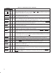
The terminals in Table 2–3 through Table 2–8 are grouped in tables by functionality, such as PCI system function
and power supply function. The terminal numbers are also listed for convenient reference.
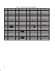
Table 2–3. Power Supply Terminals
TERMINAL
I/O
DESCRIPTION
NAME NO.
I/O
DESCRIPTION
GND
1, 11, 24, 30,
50, 60, 75, 83,
94
I Device ground terminals
V
CCP
6, 16, 39, 63,
87
I PCI signaling clamp voltage power input. PCI signals are clamped per the
PCI Local Bus Specification
.
3.3 V
CC
9, 13, 20, 35,
46, 55, 70, 80,
91, 96
I 3.3-V power supply terminals