
Datasheet
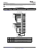


Table Of Contents
C
L
(see Note A)
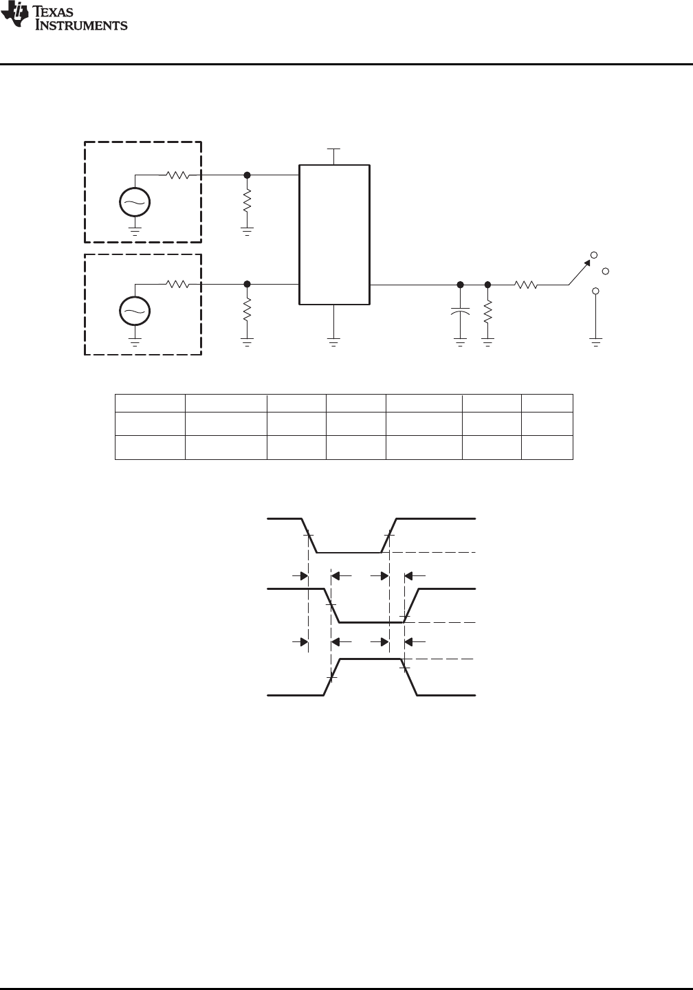
TEST CIRCUIT
S1
2 × V
D
D
Open
GND
R
L
R
L
NOTES: A. C
L
includes probe and jig capacitance.
B. Waveform 1 is for an output with internal conditions such that the output is low, except when disabled by the output control.
Waveform 2 is for an output with internal conditions such that the output is high, except when disabled by the output control.
C.
All input pulses are supplied by generators having the following characteristics:PRR ≤
10 MHz, Z
O
= 50 Ω, t
r
≤ 2.5 ns, t
f
≤ 2.5 ns.
D. The outputs are measured one at a time, with one transition per measurement.
E. t
PLZ
and t
PHZ
are the same as t
dis
.
F. t
PZL
and t
PZH
are the same as t
en
.
50 Ω
V
G1
V
DD
DUT
50 Ω
V
IN
50 Ω
V
G2
50 Ω
V
I
TEST
R
L
S1 V
∆
C
L
V
DD
V
in
t
PLZ
/t
PZL
2 × V
DD
200 Ω GND 4 pF 0.3 V
Input Generator
Input Generator
V
O
t
PHZ
/t
PZH
GND 200 Ω V
D
D
4 pF 0.3 V
t
PZL
V
OH
- 0.3 V
VOLTAGE WAVEFORMS
ENABLE AND DISABLE TIMES
V
CC
/2
V
DC
/2
Output Control
(V
IN
)
V
OH
V
OL
+ 0.3 V
V
OH
V
OL
0 V
t
PZH
t
PLZ
t
PHZ
Output
Waveform 2
S1 at GND
(see Note B)
Output
Waveform 1
S1 at 2 x V
C
C
(see Note B)
V
OL
V
O
V
SEL
V
O
3.3 V ± 0.3 V
3.3 V ± 0.3 V
1.65 V1.65 V
3.33 V
TS3DDR3812
www.ti.com
SCDS314A –FEBRUARY 2011– REVISED MARCH 2011
PARAMETER MEASUREMENT INFORMATION
Enable and Disable Times
Figure 5. Test Circuit and Voltage Waveforms
Copyright © 2011, Texas Instruments Incorporated Submit Documentation Feedback 7
Product Folder Link(s) :TS3DDR3812