
Datasheet
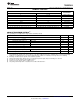
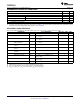


Table Of Contents
TS3DDR3812
www.ti.com
SCDS314A –FEBRUARY 2011– REVISED MARCH 2011
SWITCHING CHARACTERISTICS
Over recommended operation free-air temperature range, V
CC
= 3.3 V ± 0.3 V, R
L
= 200 Ω, C
L
= 4 pF (unless otherwise
noted) (see Figure 5 and Figure 6)
FROM TO
PARAMETER MIN TYP
(1)
MAX UNIT
(INPUT) (OUTPUT)
t
pd
(2)
A or B,C B,C or A 40 ps
t
PZH
, t
PZL
SEL1 A
0-5
or B
0-5
, C
0-5
2 7 ns
SEL2 A
6-11
or B
6-11
, C
6-11
2 7 ns
t
PHZ
, t
PLZ
SEL1 A
0-5
or B
0-5
, C
0-5
2 5 ns
SEL2 A
6-11
or B
6-11
, C
6-11
2 5 ns
t
sk(o)
(3)
A or B,C B, C or A 6 30 ps
t
sk(p)
(4)
A or B, C B, C or A 6 30 ps
(1) All typical values are at V
CC
= 3.3V (unless otherwise noted), T
A
= 25°C.
(2) The propagation delay is the calculated RC time constant of the typical ON-State resistance of the switch and the specified load
capacitance when driven by an ideal voltage source (zero output impedance).
(3) Output skew between center port (A
5
, A
6
) and any other channel.
(4) Skew between opposite transitions of the same output |t
PHL
– t
PLH
|
DYNAMIC CHARACTERISTICS
over recommended operating free-air temperature range, V
CC
= 3.3 V ± 0.3 V (unless otherwise noted)
PARAMETER TEST CONDITIONS TYP
(1)
UNIT
X
TALK
R
L
= 50 Ω, f = 250 MHz (see Figure 8) –43 dB
O
IRR
R
L
= 50 Ω, f = 250 MHz (see Figure 9) –42 dB
BW R
L
= 50 Ω, Switch ON (see Figure 7) 1.675 GHz
(1) All Typical Values are at V
CC
= 3.3 V (unless otherwise noted), T
A
= 25°C.
Copyright © 2011, Texas Instruments Incorporated Submit Documentation Feedback 5
Product Folder Link(s) :TS3DDR3812