
Datasheet
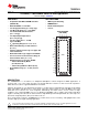
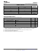
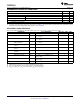


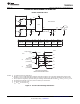


Table Of Contents
TS3DDR3812
SCDS314A –FEBRUARY 2011– REVISED MARCH 2011
www.ti.com
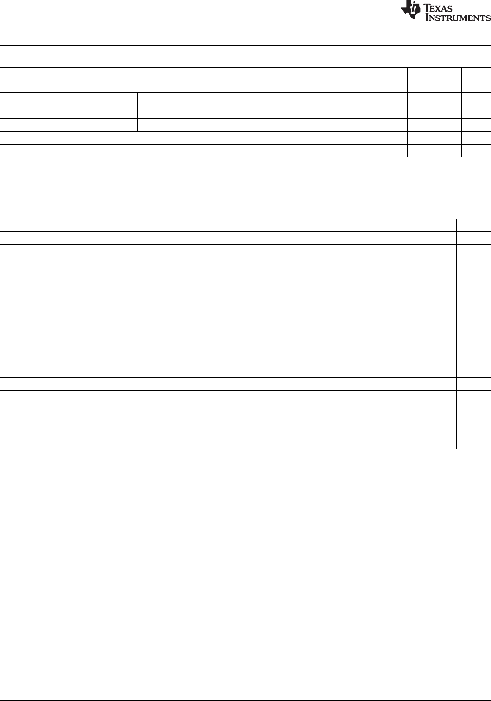
RECOMMENDED OPERATING CONDITIONS
(1)
MIN MAX UNIT
V
CC
Supply voltage 3 3.6 V
V
IH
High-level control input voltage SEL1, SEL2 2 5.5 V
V
IL
Low-level control input voltage SEL1, SEL2 0 0.8 V
V
IN
Input voltage SEL1, SEL2 0 5.5 V
V
I/O
Input/Output voltage 0 V
CC
V
T
A
Operating free-air temperature –40 85 °C
(1) All unused control inputs of the device must be held at V
DD
or GND to ensure proper device operation. Refer to the TI application report,
Implications of Slow or Floating CMOS Inputs, literature number SCBA004
ELECTRICAL CHARACTERISTICS
over recommended operating free-air temperature range, V
CC
= 3.3 V ± 0.3 V (unless otherwise noted)
PARAMETER TEST CONDITIONS
(1)
MIN TYP
(2)
MAX UNIT
V
IK
Digital input clamp voltage SEL1, SEL2 V
CC
= 3.6 V, I
IN
= –18 mA –1.2 –0.8 V
R
ON
ON-state resistance A, B, C V
CC
= 3 V, 1.5 V ≤ V
I/O
≤ V
CC
, 8 12 Ω
I
I/O
= -40 mA
R
ON(flat)
(3)
ON-state resistance flatness A, B, C V
CC
= 3 V, V
I/O
= 1.5 V and V
CC
, 1.5 Ω
I
I/O
= –40 mA
ΔR
ON
(4)
On-state resistance match A, B, C V
CC
= 3 V, 1.5 V ≤ V
I/O
≤ V
CC
, 0.4 1 Ω
between channels
I
I/O
= –40 mA
I
IH
Digital input high leakage SEL1, SEL2 V
CC
= 3.6 V , V
IN
= V
DD
±1 µA
current
I
IL
Digital input low leakage SEL1, SEL2 V
CC
= 3.6 V, V
IN
= GND ±1 µA
current
I
OFF
Leakage under power off All outputs V
CC
= 0 V, V
I/O
= 0 to 3.6 V, V
IN
= 0 to 5.5 V ±1 µA
conditions
C
IN
Digital input capacitance SEL1, SEL2 f = 1 MHz, V
IN
= 0 V 2.6 3.2 pF
C
OFF
Switch OFF capacitance A, B, C f = 1 MHz, V
I/O
= 0 V, Output is open, 2 pF
Switch is OFF
C
ON
Switch ON capacitance A, B, C f = 1 MHz, V
I/O
= 0 V, Output is open, 5.6 pF
Switch is ON
I
CC
V
CC
supply current V
CC
= 3.6 V, I
I/O
= 0, V
IN
= V
DD
or GND 300 400 µA
(1) V
I
, V
O
, I
I
, and I
O
refer to I/O pins, V
IN
refers to the control inputs
(2) All typical values are at V
CC
= 3.3V (unless otherwise noted), T
A
= 25°C
(3) R
ON(FLAT)
is the difference of R
ON
in a given channel at specified voltages.
(4) ΔR
ON
is the difference of R
ON
from center port (A
5
, A
6
) to any other ports.
4 Submit Documentation Feedback Copyright © 2011, Texas Instruments Incorporated
Product Folder Link(s) :TS3DDR3812