Using the TPS92001EVM-628 User's Guide Literature Number: SLUU897 March 2012
User's Guide SLUU897 – March 2012 Dimmable LED Lighting Driver Controller 1 Introduction The TPS92001EVM-628 evaluation module is a constant-current, dimmable LED driver. It is designed to drive 9 LEDs at 330 mA and is rated for an AC input of 105 VRMS to 135 VRMS. 2 Description The TPS92001/2 family of general LED lighting PWM controllers contains control and drive circuitry required for off-line isolated or non-isolated LED lighting applications.
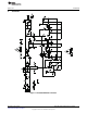
Schematic www.ti.com 4 Schematic Figure 1.
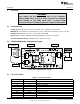
Test Setup 5 www.ti.com Test Setup WARNING High voltages that may cause injury exist on this evaluation module (EVM). Please ensure all safety procedures are followed when working on this EVM. Never leave a powered EVM unattended. The use of isolated equipment is highly recommended. 5.1 Test Equipment Voltage Source: 105 VRMS to 135 VRMS isolated AC source capable of at least 20 W. Multimeters: Two voltmeters for measuring up to 35 VDC each and two ammeters for up to 1 A each.
Test Procedure www.ti.com 6 Test Procedure All tests should use the set up described in Section 5 of this user guide. WARNING High voltage levels are present on this evaluation module whenever it is energized. Proper precautions must be observed whenever working with this module. Serious injury can occur if proper safety procedures are not followed. 6.1 Line/Load Regulation and Efficiency Measurement Procedure 1. 2. 3. 4. Connect EVM per Figure 2 above.
Performance Data and Typical Characteristic Curves 7 www.ti.com Performance Data and Typical Characteristic Curves Figure 3 through Figure 28 present typical performance curves for TPS92001EVM-628. Unless otherwise specified the following test conditions are required: 1. Use LED load module PR916 set for 9 LED load. 2. Figure 6 through Figure 28 input set to 120 VAC nominal. 3. Triac dimmer used is Leviton Cat No 6684 or equivalent. 7.
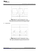
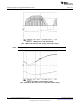
Performance Data and Typical Characteristic Curves www.ti.com 7.3 Input Voltage vs. Output Current Output current (mA) Input voltage vs. Output current 400 390 380 370 360 350 340 330 320 310 300 105 110 115 120 125 Input voltage (VAC) 130 135 Figure 5. Output Current Variation (with respect to input voltage) Turn-on angle vs. Iout 350 300 Iout (mA) 250 200 150 100 50 0 5 25 45 65 85 105 Turn-on angle (degrees) 125 145 165 Figure 6.
Performance Data and Typical Characteristic Curves 7.4 www.ti.com Output Ripple Figure 7. Output Ripple (Ch1-LED current Ch2- rectified line voltage Ch3- Q2 drain) 7.5 Input Waveforms Figure 8.
Performance Data and Typical Characteristic Curves www.ti.com 7.6 Current Fdbk Signal and Switch Node Voltage Figure 9. Current Sense and Switching Node Waveform (peak line) (Ch1- LED current Ch2- Q2 current sense Ch3- Q2 drain voltage) 7.7 Current Sense Figure 10.
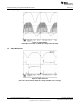
Performance Data and Typical Characteristic Curves 7.8 www.ti.com Triac Dimmer Waveforms Figure 11. LED Current vs. Q2 Switch Node (Ch1- LED current Ch2- Q2 drain voltage Ch3- bulk voltage) NOTE: LED current highly filtered. Figure 12.
Performance Data and Typical Characteristic Curves www.ti.com Figure 13. Triac Holding Current (2.5-ms Triac on time) (Ch1- LED current Ch2- bulk voltage Ch3- Q4 source voltage) Figure 14.
Performance Data and Typical Characteristic Curves 7.9 www.ti.com Triac Phase Waveforms Figure 15. Dummy Load Conduction Time vs. Dimmer Setting (Ch1- Line current Ch2- bulk voltage Ch3- Q4 source voltage) Figure 16. Dummy Load Conduction Time vs.
Performance Data and Typical Characteristic Curves www.ti.com Figure 17. Dummy Load Conduction Time vs. Dimmer Setting (Ch1- line current Ch2- bulk voltage Ch3- Q4 source voltage ) Figure 18. Dummy Load Conduction Time vs.
Performance Data and Typical Characteristic Curves www.ti.com Figure 19. Dummy Load Conduction Time vs. Dimmer Setting (Ch1- line current Ch2- bulk voltage Ch3- Q4 source voltage ) Figure 20. Dummy Load Conduction Time vs.
Performance Data and Typical Characteristic Curves www.ti.com Figure 21. LED Current vs. Triac Conduction Time (Ch1- LED current Ch2- bulk voltage Ch3- U2-1 voltage waveform) NOTE: U2-1 is Q2 averaged current feedback. Figure 22. LED Current vs. Triac Conduction Time (Ch1- LED current Ch2- bulk line voltage Ch3- U2-1 voltage waveform) NOTE: U2-1 is Q2 averaged current feedback.
Performance Data and Typical Characteristic Curves www.ti.com Figure 23. LED Current vs. Triac Conduction Time (Ch1- LED current Ch2- bulk voltage Ch3- U2-1 voltage waveform) NOTE: U2-1 is Q2 averaged current feedback. Figure 24. LED Current vs. Triac Conduction Time (Ch1- LED current Ch2- bulk voltage Ch3- U2-1 voltage waveform) NOTE: U2-1 is Q2 averaged current feedback.
Performance Data and Typical Characteristic Curves www.ti.com Figure 25. LED Current vs. Triac Conduction Time (Ch1- LED current Ch2- bulk voltage Ch3- U2-1 voltage waveform) NOTE: U2-1 is Q2 averaged current feedback. Figure 26. LED Current vs. Triac Conduction Time (Ch1- LED current Ch2- bulk voltage Ch3- U2-1 voltage waveform) NOTE: U2-1 is Q2 averaged current feedback.
Performance Data and Typical Characteristic Curves www.ti.com Figure 27. LED Current vs. Triac Conduction Time (Ch1- LED current Ch2- bulk voltage Ch3- U2-1 voltage waveform) NOTE: U2-1 is Q2 averaged current feedback. Figure 28. LED Current vs. Triac Conduction Time (Ch1- LED current Ch2- bulk voltage Ch3- U2-1 voltage waveform) NOTE: U2-1 is Q2 averaged current feedback.
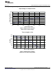
www.ti.com 8 TPS92001EVM-628 Assembly Drawing and PCB layout TPS92001EVM-628 Assembly Drawing and PCB layout The following figures (Figure 29 through Figure 32) show the design of the TPS92001EVM-628 printed circuit board. Figure 29. Assembly Drawing (top view) Figure 30.
TPS92001EVM-628 Assembly Drawing and PCB layout www.ti.com Figure 31. Top Copper (top view) Figure 32.
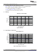
List of Materials www.ti.com 9 List of Materials The TPS92001EVM-628 component's list according to the schematic shown in Figure 1. Table 3. TPS92001EVM-628 List of Materials QTY REF DES DESCRIPTION PART NUMBER MFR 2 C1,C12 Capacitor, leaded, metalized film, 400 VDC, 125°C, 20 ±%, 0.1 µF, 0.310 inch x 0.310 inch B32529D6104J or B32559C6104K001 Epcos 1 C10 Capacitor, ceramic, 25 V, X7R, 10%, 1.0 µF, 0805 Std Std 1 C11 Capacitor, ceramic, 10 V, X7R, 10%, 0.
List of Materials www.ti.com Table 3. TPS92001EVM-628 List of Materials (continued) QTY REF DES DESCRIPTION PART NUMBER MFR 1 R1 Resistor, 1/4 W, ±5%, 1.0 kΩ, 1206 Std Std 1 R10 Resistor, chip, 1/16 W, 1%, 4.32 kΩ, 0603 Std Std 1 R2 Resistor, 1/4 W, ±5%, 604 kΩ, 1206 Std Std 1 R3 Resistor, chip, 1/16 W, 1%, 5.11 kΩ, 0603 Std Std 1 R4 Resistor, chip, 1/16 W, 1%, 10 Ω, 0603 Std Std 1 R5 Resistor, SM, 3/4 W, 1%, 2.7 Ω, 2010 Std Std 1 R7 Resistor, chip, 1/16 W, 1%, 4.
Evaluation Board/Kit Important Notice Texas Instruments (TI) provides the enclosed product(s) under the following conditions: This evaluation board/kit is intended for use for ENGINEERING DEVELOPMENT, DEMONSTRATION, OR EVALUATION PURPOSES ONLY and is not considered by TI to be a finished end-product fit for general consumer use. Persons handling the product(s) must have electronics training and observe good engineering practice standards.
EVALUATION BOARD/KIT/MODULE (EVM) ADDITIONAL TERMS Texas Instruments (TI) provides the enclosed Evaluation Board/Kit/Module (EVM) under the following conditions: The user assumes all responsibility and liability for proper and safe handling of the goods. Further, the user indemnifies TI from all claims arising from the handling or use of the goods.
FCC Interference Statement for Class B EVM devices This equipment has been tested and found to comply with the limits for a Class B digital device, pursuant to part 15 of the FCC Rules. These limits are designed to provide reasonable protection against harmful interference in a residential installation. This equipment generates, uses and can radiate radio frequency energy and, if not installed and used in accordance with the instructions, may cause harmful interference to radio communications.
【Important Notice for Users of this Product in Japan】 】 This development kit is NOT certified as Confirming to Technical Regulations of Radio Law of Japan If you use this product in Japan, you are required by Radio Law of Japan to follow the instructions below with respect to this product: 1. 2. 3. Use this product in a shielded room or any other test facility as defined in the notification #173 issued by Ministry of Internal Affairs and Communications on March 28, 2006, based on Sub-section 1.
EVALUATION BOARD/KIT/MODULE (EVM) WARNINGS, RESTRICTIONS AND DISCLAIMERS For Feasibility Evaluation Only, in Laboratory/Development Environments. Unless otherwise indicated, this EVM is not a finished electrical equipment and not intended for consumer use.
IMPORTANT NOTICE Texas Instruments Incorporated and its subsidiaries (TI) reserve the right to make corrections, enhancements, improvements and other changes to its semiconductor products and services per JESD46, latest issue, and to discontinue any product or service per JESD48, latest issue. Buyers should obtain the latest relevant information before placing orders and should verify that such information is current and complete.