
Datasheet
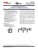
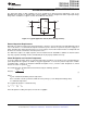


_
+
Current
Sense
LeakageNull
ControlCircuit
R1
R2
V
(IN)
GND
V
(OUT)
ILIM
Bandgap
Reference
V =1.205V
ref
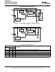
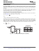
_
+
Current
Sense
LeakageNull
ControlCircuit
R1
R2
V
(IN)
GND
V
(OUT)
ILIM
Bandgap
Reference
V =1.205V
ref
FB
TPS71501-Q1
TPS71525-Q1, TPS71530-Q1
TPS71533-Q1, TPS71550-Q1
SGLS272G –OCTOBER 2004–REVISED JULY 2013
www.ti.com
FUNCTIONAL BLOCK DIAGRAMS
Figure 1. Functional Block Diagram—Adjustable Version
Figure 2. Functional Block Diagram—Fixed Version
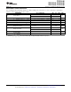
Table 1. Terminal Functions
TERMINAL
NO. DESCRIPTION
NAME
FIXED ADJ.
FB 1 Adjustable version only. This terminal is used to set the output voltage.
NC 1 No connection
GND 2 2 Ground
NC 3 3 No connection
IN 4 4 Input supply.
OUT 5 5 Output of the regulator, any output capacitor ≥ 0.47 μF can be used for stability.
4 Submit Documentation Feedback Copyright © 2004–2013, Texas Instruments Incorporated
Product Folder Links: TPS71501-Q1 TPS71525-Q1 TPS71530-Q1 TPS71533-Q1 TPS71550-Q1